CdSe-based quantum-dot light-emitting diodes (QLEDs) have been extensively explored for applications in displays due to their unique merits of self-emission, high brightness, tunable emission color, wide color gamut, high efficiency, flexible and low-cost solution processability. Consequently, they have been hotly investigated as one of the substitutes for Organic light-emitting diodes (OLEDs) for next-generation displays.
Associate Professor Shuming Chen and his team from the Department of Electronic and Electrical Engineering at the Southern University of Science and Technology (SUSTech) developed the photopatternable color-converting cavity to realize ultrahigh resolution and high brightness QLED displays. Their research, entitled “Ultrahigh Resolution Pixelated Top-Emitting Quantum-Dot Light-Emitting Diodes Enabled by Color-Converting Cavities,” was recently published as the cover article in Small Methods. It was also selected as the Editor’s Choice.
To realize full-color QLED displays, the quantum dots (QDs) have to be finely patterned so that pixelated red (R), green (G), and blue (B) QDs are arranged in a horizontal side-by-side manner. But the colloidal QDs can only be deposited and patterned by a solution process, which remains one of the challenging tasks that hinder the development of QLED displays.
Among the proposed methods, the most common technologies are ink-jet printing, transfer printing, QD photolithography, etc., which directly pattern the quantum dots. After three patterning processes, the quantum dots will inevitably be destroyed, making the QLED performance lower. Instead of patterning the QDs directly, the red, green, and blue emission can also be obtained by filtering the white emission with a pixelated color filter (CF) array. But the introduction of CF reduces over 70% of the brightness.
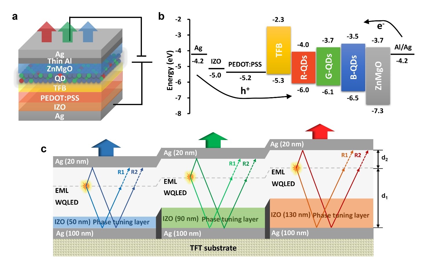
Figure 1. Device structure, working principle, and patterning method of a pixelated QLED array. (a) Schematic device structure. (b) Energy level alignment of a top-emitting QLED equipped with a color-converting cavity, in which metallic Ag films serve as electrodes and reflection mirrors for the cavity device, and IZO functions as a phase tuning layer. (c) Schematic illustration of a full-color QLED array.
To address the aforementioned challenges, the research team developed a CF-free, QD-patterning-free, and large-area compatible method for realizing ultrahigh resolution and high brightness QLED displays. Unlike previously demonstrated techniques, they realized ultrahigh resolution pixelated red, green, and blue emission by developing the photopatternable color-converting cavities.
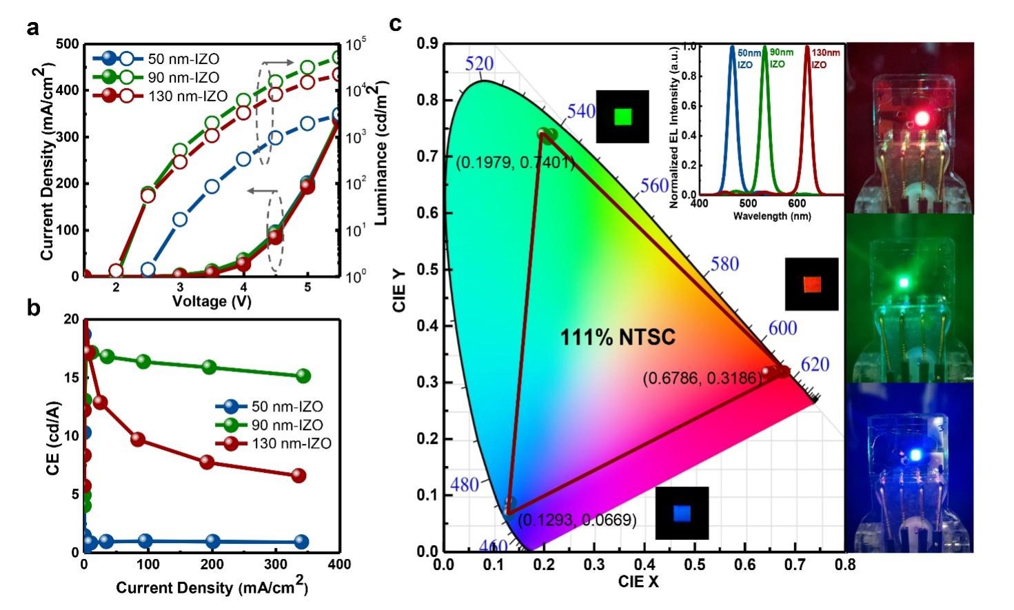
Figure 2. Performance of the converted emission. (a) The current density-voltage-luminance (J-V-L). (b) The current efficiency-current density (CE-J) characteristics. (c) The color coordinates and color triangle of the converted red, green, and blue emission. Inset of (c) displays the spectra and the photos of the converted red, green, and blue emissions.
By varying the thicknesses of the phase tuning layers through a photolithographic process, the optical interference of the cavities can be manipulated. Consequently, the cavities can selectively convert the unpatterned QD white emission as saturated red, green, and blue emissions with a brightness of 22170, 51930, and 3064 cd/m2 at 5.5 V, respectively. Benefitting from the very narrow bandwidth of the QD emission, the cavities can output saturated colors with a small color-talk. The cavities can also modulate the emission color as well as the excitonic energy transfer among QDs.
The developed method enables the realization of ultra-high-density red, green, and blue emissions for a display with a resolution of ~1700 Pixels Per Inch (PPI) that can be improved to over 8000 PPI, and a color gamut of 111% National Television Standards Committee (NTSC). Together with the advantages of QD-patterning-free, CF-free, top-emitting, and high brightness, the demonstrated method could find potential applications in various displays ranging from cell phones to emerging virtual reality (VR) and augmented reality (AR) displays.
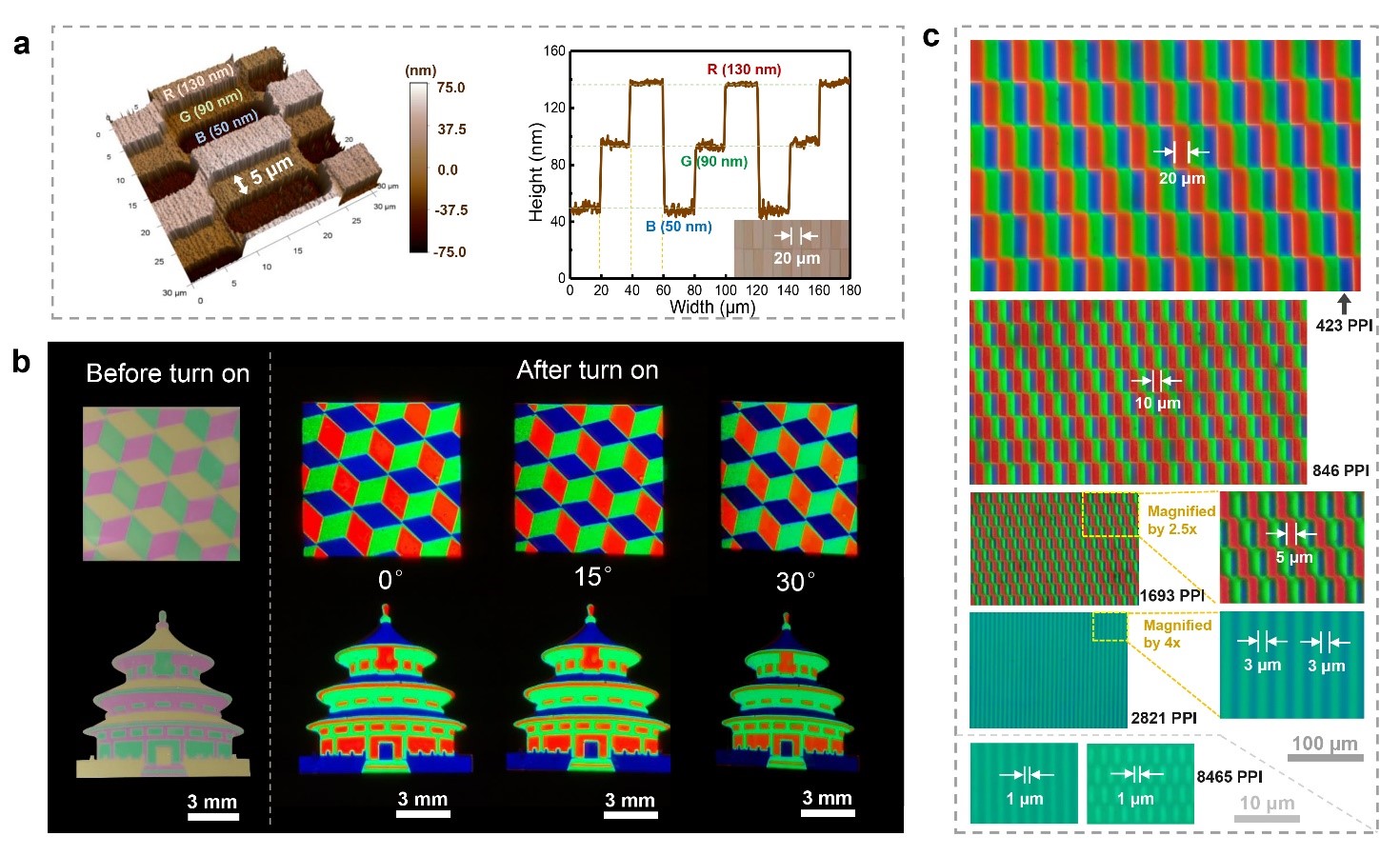
Figure 3. Demonstration of ultrahigh resolution pixelated QLED arrays. (a) The Atomic Force Microscopic (AFM) image and the step profile of the patterned IZO phase tuning layers with a width of 5 and 20 μm. (b) Photos of two full-color QLEDs that display the patterns of the cubical pixels and the Beijing temple of heaven, respectively. (c) Pixelated QLED arrays with square pixel shape and subpixel size from 20 to 5 μm, and line shape with subpixel size from 3 to 1 μm.
Lianna Chen, a master’s student from SUSTech, is the first author of the paper. Zhiyuan Qin, a master’s student from SUSTech, is the second author. Associate Professor Shuming Chen is the corresponding author.
This research was supported by the National Natural Science Foundation of China (NSFC).
Paper link: https://onlinelibrary.wiley.com/doi/10.1002/smtd.202101090
To read all stories about SUSTech science, subscribe to the monthly SUSTech Newsletter.
Proofread ByAdrian Cremin, Yingying XIA
Photo By