The display industry is one of the most important parts of the whole electronics industry in the world. Metal halide perovskites have recently attracted much attention as promising materials for display applications, owing to their wide color gamut, facile color tunability, and excellent carrier mobility. To date, one of the main challenges of PeLEDs is to achieve high-performance blue electroluminescence.
Associate Professor Kai Wang’s team from the Department of Electrical and Electronic Engineering at the Southern University of Science and Technology (SUSTech) has recently made a series of research developments in the field of perovskite LEDs (PeLEDs) and perovskite single crystal thin films (SCTFs). They published three academic papers in top international journals, including ACS Energy Letters, Nano-Micro Letters, and Advanced Science.
Their first paper, entitled “Efficient CsPbBr3 Nanoplatelet-Based Blue Light-Emitting Diodes Enabled by Engineered Surface Ligands,” was published as the cover article in ACS Energy Letters. Their study demonstrated an efficient synthesis strategy leading to short-ligand (butylamine and myristic acid)-capped CsPbBr3 Nanoplatelet (NPL) with almost unaltered emission characteristics by introducing ammonium bromide (NH4Br) to effectively control the crystal growth kinetics and passivate the surface defects. CsPbBr3 NPLs with short ligands exhibit enhanced charge transport ability and give rise to a remarkable electroluminescence efficiency of 2% (λ=463 nm), a record for NPLs-based blue PeLEDs.
Figure 1. (a) Schematic of the formation of NPLs after the introduction of NH4Br. (b) TEM and HRTEM images of NPLs. (c) Comparison of the performance of blue PeLEDs based on NPLs.
Haoran Wang, a visiting Ph.D. student from Harbin Institute of Technology (Shenzhen), is the first author of this paper. Associate Prof. Kai Wang and Prof. Weiwei Zhao from Harbin Institute of Technology (Shenzhen) are the co-corresponding authors.
The second paper, entitled “High-Performance Blue Quasi-2D Perovskite Light-Emitting Diodes via Balanced Carrier Confinement and Transfer,” was published in Nano-Micro Letters. Their study showed that the appropriate carbon chain length of tributylphosphine oxide (TBPO) could simultaneously offer good carrier confinement for the massive radiative recombination within the perovskites and efficient carrier transfer in quasi-2D perovskites for high emission efficiency. With these benefits, high-efficient blue PeLEDs with an EQE of 11.5% (λ=488 nm) have been achieved, which is among the best-performing blue PeLEDs.
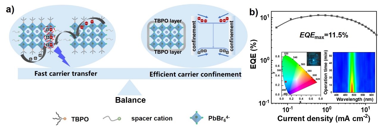
Figure 2. (a) TBPO combines charge transport and confinement. (b) EQE-J curves of blue PeLED.
Zhenwei Ren, a visiting postdoctoral from the University of Hong Kong (HKU), is the first author of this paper. Associate Prof. Kai Wang, Prof. Rui Chen from SUSTech, and Prof. Wallace C. H. Choy from HKU are the co-corresponding authors.
Perovskite single-crystal materials, with a variety of merits such as no grain boundaries, low trap densities, long carrier lifetime, and good stability, are considered as extremely promising optoelectronic materials. However, the fabrication of large-area high-quality SCTFs with thin thickness still remains a significant challenge due to the elusive growth mechanism of this process.
The third paper, entitled “In Situ Growth Mechanism for High-Quality Hybrid Perovskite Single-Crystal Thin Films with High Area to Thickness Ratio: Looking for the Sweet Spot,” was published in Advanced Science. In this study, the researchers revealed a sweet spot that affects the in situ growth of perovskite single-crystal thin film on transport layers with theoretical analysis, namely low interface energy between precursor solution and transport layer, slow heating rate, and moderate precursor solution concentration. Based on these findings, a high-quality MAPbBr3 perovskite single-crystal film with an area to thickness ratio of 1.94 × 104 mm and a carrier mobility of 141 cm2V-1s-1 was prepared, which are the highest values reported in the literature in terms of MAPbBr3 perovskite single-crystal film.
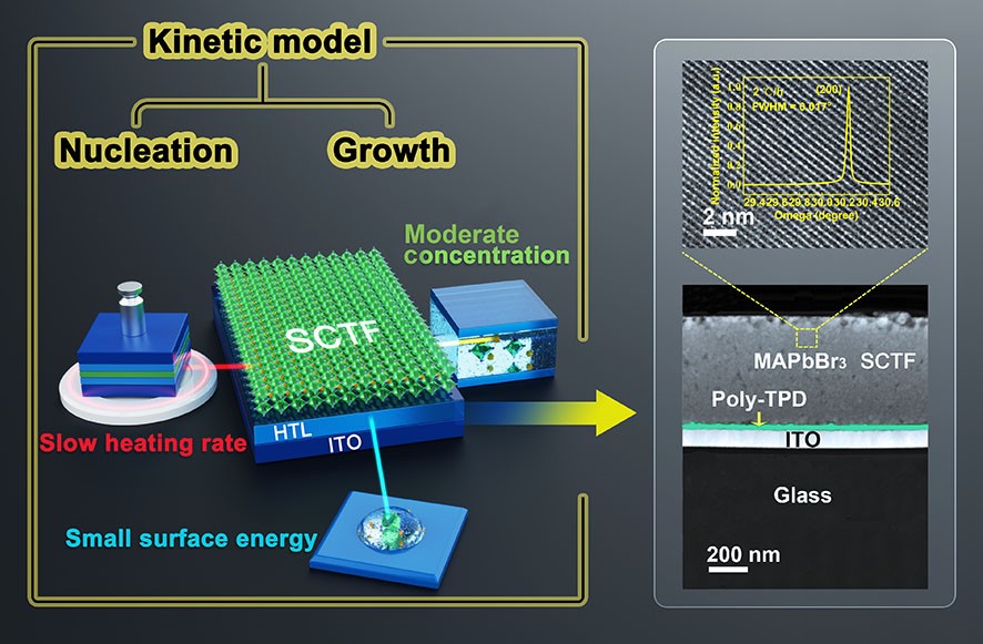
Figure 3. In situ growth mechanism for MAPbBr3 perovskite single-crystal thin films.
Xiaobing Tang, Research Assistant and now a Ph.D. student at the University of Kentucky, USA, and Zhaojin Wang, a joint Ph.D. student of SUSTech and the Harbin Institute of Technology, are the co-first authors of this paper. Associate Prof. Kai Wang, Assistant Prof. Dan Wu from Shenzhen Technology University (SZTU), and Prof. Fuqian Yang from the University of Kentucky are the co-corresponding authors.
The above studies were supported by the National Natural Science Foundation of China (NSFC), National Key Research and Development Program, Distinguished Young Scholar of Natural Science Foundation of Guangdong, Shenzhen Fundamental Research Programs, Key Laboratory of Energy Conversion and Storage Technology of Ministry of Education, Guangdong-Hong Kong-Macao Joint Laboratory for Photonic-Thermal-Electrical Energy Materials and Devices, and Guangdong University Key Laboratory for Advanced Quantum Dot Displays and Lighting.
Paper links (In order of appearance above):
ACS Energy Letters: https://pubs.acs.org/doi/abs/10.1021/acsenergylett.1c02642
Nano-Micro Letters: https://link.springer.com/article/10.1007/s40820-022-00807-7
Advanced Science: https://onlinelibrary.wiley.com/doi/full/10.1002/advs.202104788
To read all stories about SUSTech science, subscribe to the monthly SUSTech Newsletter.
Proofread ByAdrian Cremin, Yingying XIA
Photo By