Power management integrated circuits have been essential parts for every electronic system. Higher efficiency, higher power density, and compact size are in high demands to reduce the system volume and extend the battery life, but still facing challenges in nowadays technologies.
Assistant Professor Junmin Jiang’s research group from the Department of Electrical and Electronics Engineering at the Southern University of Science and Technology (SUSTech), in collaboration with the Chinese University of Hong Kong, Shenzhen (CUHK-Shenzhen) and the Hong Kong University of Science and Technology (HKUST), has made a number of developments in the field of power management chips, such as RF envelope trackers and fully integrated switched capacitor converters.
Firstly, in the field of RF envelope tracker, the application and design challenges in next-generation communication technology are summarized and prospected. The transfer function and stability of the envelope tracker design are analyzed. In the field of fully integrated switched capacitor converters, the idea of multiphase sharing is proposed, which will greatly improve the current density of the converter.
The research group has published three papers in IEEE Transactions on Circuits and Systems II: Express Briefs (T-CAS II), an international high-level journal in the field of integrated circuits.
Their first paper published in T-CAS II was entitled “Design Techniques for High-Efficiency Envelope-Tracking Supply Modulator for 5th Generation Communication”.
The fifth-generation communication technology 5G (5th Generation) is the basic technology of the next-generation industrial revolution, with comprehensive performance improvements, including faster speed and lower latency. However, the high peak-to-average power ratio (PAPR) of around 10 dB in 5G communication severely reduces the efficiency of RF power amplifiers, resulting in large energy loss and affecting the battery life of mobile devices.
As shown in Figure 1, the power amplifier system is mainly composed of an RF power amplifier and power modulator. The traditional solution uses a constant voltage power supply, and the overall efficiency of the power amplifier system is only 10%. The power modulator in the Envelope Tracking (ET) system tracks the envelope signal of the RF signal, which can increase the overall efficiency to 30-40%, thereby prolonging the standby time. It is the core technology in the current high-performance RF power amplifier system.

Figure 1. Conventional power supply for a power amplifier (PA) and supply modulator powered PA
5G communication has challenging requirements for the envelope tracking power modulators, which need to simultaneously achieve efficiencies greater than 80%, bandwidths around 1GHz, output voltage ranges from as low as 1V to as high as 6V, and output power of several watts. To address these challenges, power supply modulators for envelope tracking typically employ a hybrid structure combining linear amplifiers with switching converters. The basic idea is to use a high-bandwidth linear amplifier to provide high-frequency energy and a limited bandwidth but high-efficiency switching converter to provide low-frequency energy.
However, the bandwidth of the 5G signal is as high as 100MHz/200MHz, and the traditional power modulator can no longer meet this requirement. Therefore, this paper systematically expounds on the challenges of 5G communication, the most advanced technologies that can be used, and the advantages and disadvantages of these technologies. The content covers Architectural innovations, multi-level topology implementations of switching converters, fast response control and boost-buck function implementations, bandwidth extension methods for linear amplifiers, and system testing guidelines.
Prof. Xun Liu at CUHK-Shenzhen is the first author of this paper. Prof. Junmin Jiang at SUSTech is the corresponding author.
Figure 2. Comparison table of difference strategies in supply modulators
Creating a new model to predict and guide current and voltage loop designs
In their second paper, “Loop Analysis and Stability Considerations of Hybrid PA Supply Modulators,” Prof. Jiang’s group looks at a method to model and compensate for both the current and voltage loops.
The radio-frequency (RF) power amplifiers (PA) are one of the most power-hungry components in mobile phones. The PA has low efficiency because the input RF signal of the PA has a changing envelope. If the supply modulator provides a constant supply voltage to the PA, the energy between the supply voltage and the envelope is wasted. This problem is becoming more severe with modern communication protocols as the peak-to-average power ratio (PAPR) increases.
To solve this problem, the ET technique in supply modulators has been developed for decades. In an ET system, the supply modulator tracks the instantaneous envelope efficiently to reduce the power overhead. As the envelope is changing rapidly, its power is distributed across 100-MHz for LTE and even reaches 1-GHz for 5G NR. It is becoming more and more challenging for the supply modulator to achieve wide bandwidth and high efficiency at the same time.
The current loop design considerations in terms of bandwidth and stability are discussed. The interactions between the current loop and voltage loop are analyzed. As long as the linear amplifier is well compensated, the current loop will not affect the UGF and phase margin of the voltage loop, and the output voltage can be stable. But a low phase margin in the current loop will cause ringing in the inductor current, resulting in extra power losses. This analysis is well verified by simulations and measurements, giving a useful guideline to design a supply modulator with good stability and optimized efficiency at target bandwidth.
Prof. Xun Liu at CUHK-Shenzhen is the first author of this paper. Prof. Junmin Jiang at SUSTech is the corresponding author.

Figure 3. System models, bode plots, and transient waveforms improved by this model
Eliminating idling capacitors in multi-phase SCC design to increase current density
In their third paper, “Fully-Integrated Switched-Capacitor Converter With Capacitor Bridging for Improved Current Density,” the researchers presented a systematic method of eliminating idling capacitors in multi-phase SCC design.
Near-threshold computing puts stringent requirements on low voltage conversion ratio (VCR, or large step-down ratio) DC-DC power converters. To power up a near-threshold computing system, the power supply voltage typically has to be bridged down an input voltage from a 3 to 5V range to a voltage lower than 600mV. Hybrid converters are viable schemes to achieve a large step-down ratio. With the demand for integrating power converters fully on-chip, a switched-capacitor converter (SCC) is a favorable candidate, as both switches and capacitors are readily available.
Multiphase SCCs have idling capacitors, which limit the power of the SCC. But at the same time, the target of eliminating idling capacitors for a multiphase SCC meets many challenges. Firstly, direct implementation of the interleaving scheme would break the charging and discharging balance of the original SCC; Secondly, for multiphase SCCs and reconfigurable SCCs, flipping the drain and the source of a power transistor would cause a current leakage issue, which results in a low efficiency.
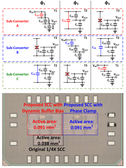
Figure 4. Schematic of proposed SCC and the chip micrograph
Interleaving capacitor bridging and phase expansion are proposed to solve the idling capacitor issue and reduce area overhead. The phase clamp method is suggested to avoid flipping drain and source issues, and minimize the leakage current. The design was fabricated in a 65nm CMOS process, and measurement results show that the current density is improved by 25% without sacrificing efficiency.
Dr. Yue Zhong at HKUST is the first author of this paper. Prof. Junmin Jiang at SUSTech is the corresponding author.
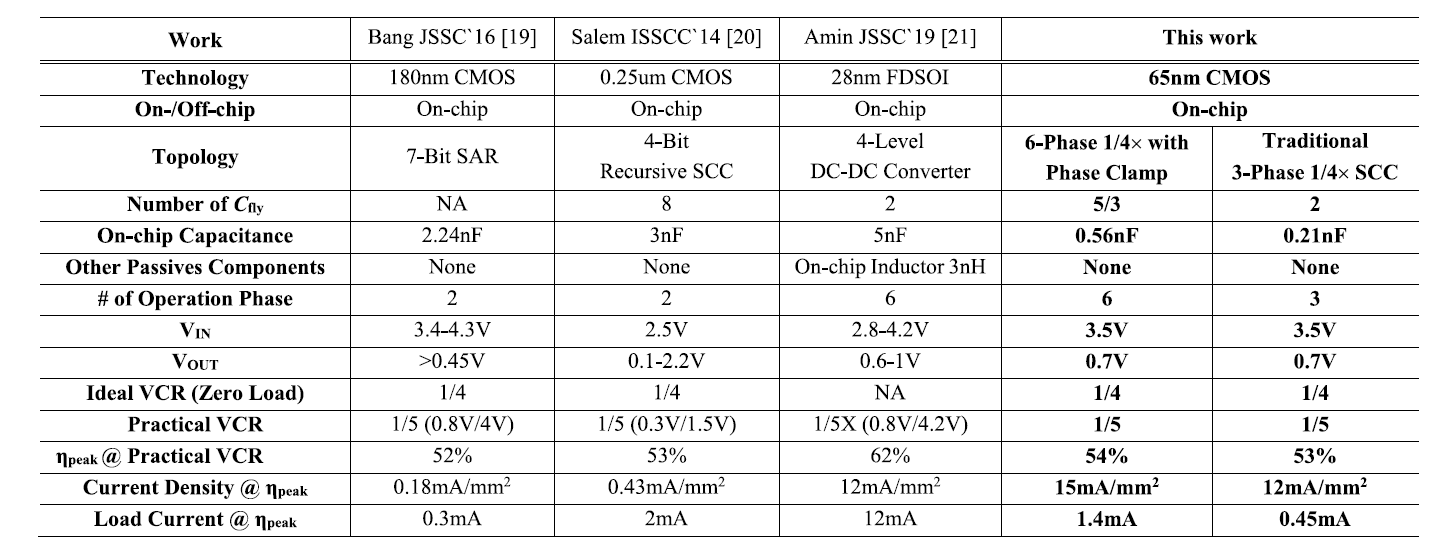
Figure 5. Comparison table with state-of-the-art works
The above research works were supported by the National Natural Science Foundation of China (NSFC), Natural Science Foundation of Guangdong Province, Shenzhen Innovation Team, and Joint Laboratory with AXS technology.
Papers links (In order of appearance above):
T-CAS II: https://ieeexplore.ieee.org/document/9751599
T-CAS II: https://ieeexplore.ieee.org/abstract/document/9803277
T-CAS II: https://ieeexplore.ieee.org/document/9790872
To read all stories about SUSTech science, subscribe to the monthly SUSTech Newsletter.
Proofread ByAdrian Cremin, Yingying XIA
Photo By