Across cloud computing and artificial intelligence applications, high-performance data centers are necessary for processing and swapping massive datasets. The growing demand for bandwidth in these data centers is pushing wireline transceivers (TRXs) to higher data rates. Yet, the data rate of TRXs is constrained by area and power consumption.
Previous studies have explored the feasibility of achieving 224-Gb/s four pulse-amplitude modulation (PAM-4) digital signal processor (DSP)-based transmitter (TX) and receiver (RX) in advanced CMOS technologies. However, these solutions consume over 820 mW/lane with a channel loss of 31-dB Nyquist. With channel loss increasing exponentially with frequency, it imposes significant equalization pressure on DSP. As a result, high interconnect loss and power consumption limits its applications in longer-distance scenarios at high data rates.
Associate Professor Quan Pan’s research team from the School of Microelectronics at the Southern University of Science and Technology (SUSTech) has recently made significant progress in the field of high-speed wireline integrated circuit design.
Their related achievements, entitled “A 2 × 56 Gb/s 0.78-pJ/b PAM-4 Crosstalk Cancellation Receiver With Active Crosstalk Extraction Technology in 28-nm CMOS”, have been published in the IEEE Journal of Solid-State Circuits (JSSC), a top journal in the field of integrated circuit design.
The IEEE 802.3 beyond 400-Gb/s Ethernet Study Group has been discussing how to enhance the data rate beyond 200 Gb/s with limited I/O ports and bandwidth. The single-ended multiple-input multiple-output (MIMO) scheme is promising to solve the issues.
The researchers proposed a single-ended MIMO PAM-4 crosstalk cancellation and signal reutilization (XTCR) medium-reach (MR) backplane RX, realizing 2 × 56 Gb/s data transmission with a pair of differential channels.

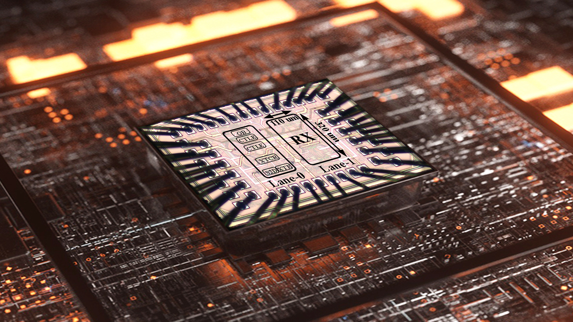
Figure 1. Single-ended MIMO crosstalk cancellation receiver chip.
Fig. 2(a) shows the area and power breakdown of the proposed receiver chip, while Fig. 2(b) and (c) show the measured eye diagram and bit error rate (BER), respectively. Compared with the traditional P-XTCR technique, the proposed A-XTCR technique achieved a 24% increase in eye height and a 15% increase in eye width, and increased the BER performance from 1e-3 to 1e-10. This receiver achieves the highest data rate of single-ended crosstalk cancellation (56 Gb/s) and the best energy efficiency (0.78 pJ/b).

Figure 2. (a) Die photo and power breakdown. (b) Measured eye diagrams. (c) BER.
Liping Zhong, a Ph.D. student at SUSTech, is the first author of the paper. Associate Professor Quan Pan is the corresponding author, and the School of Microelectronics at SUSTech is the sole affiliated unit.
This work was supported by the National Natural Science Foundation of China (NSFC) and the National Key Research and Development Program.
JSSC is a leading journal in the field of integrated circuit design and the only top journal in the JCR partition system of the Chinese Academy of Sciences in the field of integrated circuits. It is renowned for its rigorous review process, highly innovative chip design, and comprehensive and profound theoretical analysis. Submission requirements must include chip flow and world-class actual testing indicators.
Paper link: https://ieeexplore.ieee.org/document/10500691
To read all stories about SUSTech science, subscribe to the monthly SUSTech Newsletter.
Proofread ByAdrian Cremin, Yingying XIA
Photo BySchool of Microelectronics