The key scientific challenge in the atomic-scale high-precision characterization of lattice defects in low-dimensional quantum materials lies in the separation of the synthesis process from the characterization and measurement experiments. Traditional separate experimental techniques often cause sensitive samples to oxidize or hydrolyze during transfer, preventing the characterization and measurement of their intrinsic structures and properties.

Professor Junhao Lin’s research group from the Department of Physics at the Southern University of Science and Technology (SUSTech), in collaboration with domestic and international research teams, has made significant progress in the controllable synthesis of novel low-dimensional quantum materials and the atomic-scale high-precision characterization of lattice defects.
Their research includes the analysis of grain boundary (GB) defects in CVD-grown topological semimetal monolayer WTe2, the characterization of complex lattice structures in quaternary compound AuPdNaS2 nanoribbons, and the high-precision in-situ regulation of phase transition dynamics in a series of low-dimensional functional quantum materials.
The group’s related findings have been published in top journals such as Nature Materials, Nature Communications, Advanced Materials, and Science Bulletin.
Progress in understanding GBs in monolayer WTe2
Professor Junhao Lin’s group has been dedicated to addressing the challenge critical of structural instability of numerous low-dimensional functional materials. By independently developing an integrated glovebox system, they have enabled the characterization of intrinsic atomic structures in a series of air-sensitive two-dimensional quantum materials. Recently, the research group has made another breakthrough in this field. They achieved non-destructive high-precision structural characterization of the complex GB structures in large-area monolayer 1T’-WTe2 films grown using CVD technology. Their research systematically studied the associated defect-related local electronic states, revealing potential new topological GB edge states. Previously, due to extreme sensitivity to water and oxygen, achieving clear atomic imaging of GBs in monolayer 1T’ phase quantum materials had been a challenging task.
The group investigated the intrinsic GB structure and electronic properties of air-sensitive monolayer 1T’-WTe2, grown using nucleation-controlled CVD methods. By combining lateral force microscopy (LFM) with atomic-scale scanning transmission electron microscopy (STEM) imaging, they identified three main types of GB structures in bicrystal monolayer WTe2, formed through anisotropic stitching of edges. These GB structures consist of W-Te rhombi without dislocation cores. Density functional theory (DFT) calculations provided an energy-based explanation for the formation of these GB units, which serve as basic building blocks that influence the specific arrangements of GBs in continuous monolayer films.
They also observed that in polycrystalline WTe2 monolayers, the crystal domains exhibit triple orientation, interconnected through various combinations of the three basic GB structural units, resulting in different domain morphologies. More importantly, scanning tunneling microscopy/spectroscopy (STM/S) confirmed the presence of enhanced one-dimensional metallic states along the 120° twin grain boundaries (TGBs). This study provides a comprehensive model for the GB structure and physical properties of air-sensitive two-dimensional quantum materials.
The related paper, entitled “Intrinsic Grain Boundary Structure and Enhanced Defect States in Air-Sensitive Polycrystalline 1T’-WTe2 Monolayer,” has been published in Advanced Materials.
Postdoctoral Researcher Zenglong Guo from the Department of Physics at SUSTech, Associate Researcher Mengjiao Han from the Songshan Lake Materials Laboratory, doctoral student Shengfeng Zeng from the Tsinghua Shenzhen International Graduate School (Tsinghua SIGS), and doctoral student Zhouyi Yin from the Department of Physics at SUSTech are the co-first authors of the paper. Professors Bilu Liu and Xiaolong Zou from Tsinghua SIGS, Associate Professor Yue Zhao, and Professor Junhao Lin are the corresponding authors. SUSTech is the first affiliated institution of the paper.
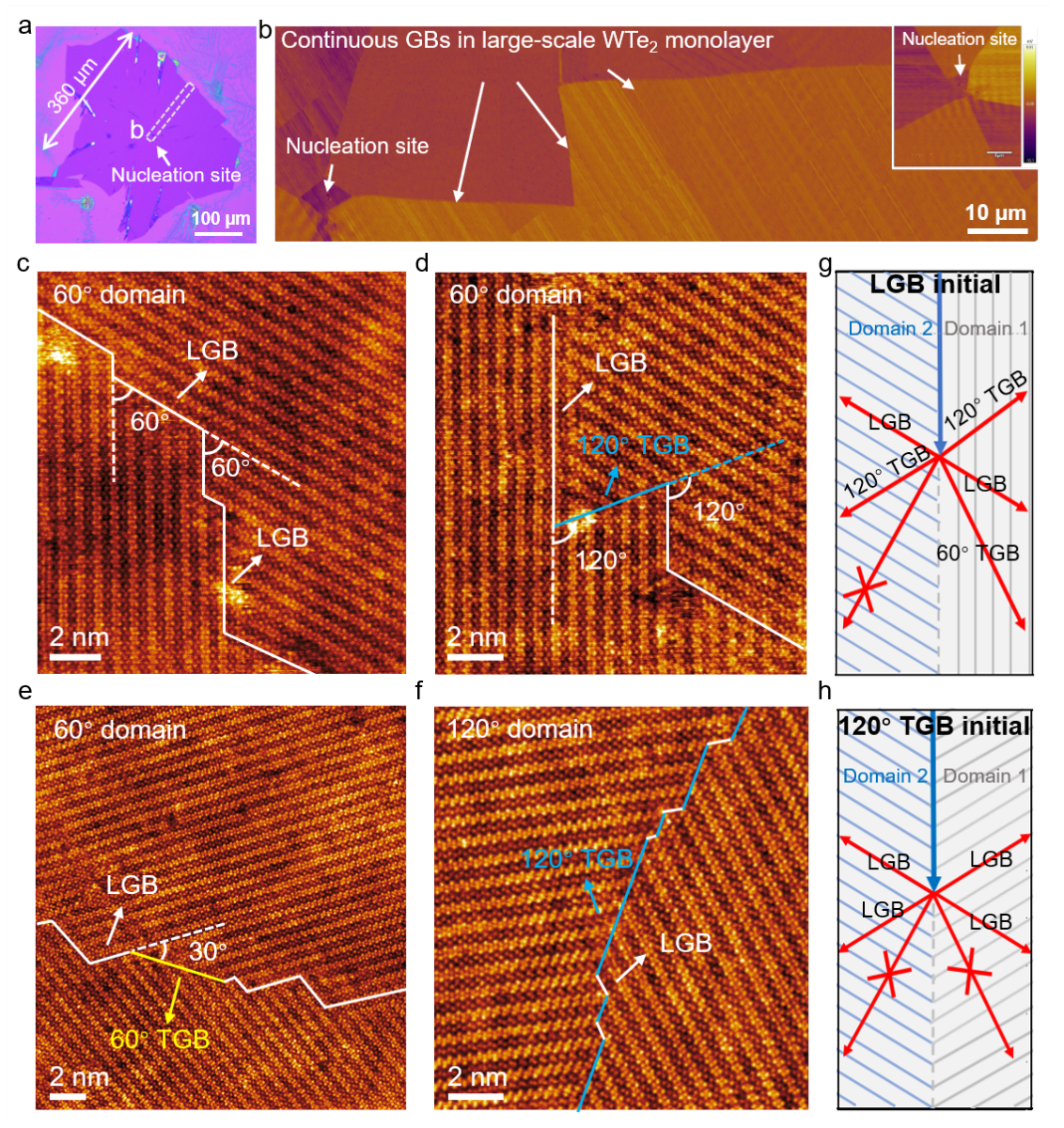
Figure 1. Nucleation-controlled CVD growth of large-area monolayer WTe2 films and their extensive intrinsic continuous GB structures
Deciphering the structure of quaternary nanoribbons
Professor Junhao Lin, in collaboration with other researchers, synthesized a novel low-dimensional quantum material, a quaternary transition metal chalcogenide (NTMC) nanoribbon AuPdNaS2, using atmospheric pressure chemical vapor deposition (APCVD). They conducted an in-depth study of its electrical transport properties. However, this low-dimensional structure comprises of four chemical elements, resulting in a highly complex crystal structure that has no recorded atomic structure model in any existing materials structure database.
The team determined the low-symmetry crystal structure of AuPdNaS2 (space group Pmcm) using advanced STEM, characterizing the atomic projections of thin-layer AuPdNaS2 crystals along three orthogonal projection axes. By applying quantitative contrast analysis techniques, where the contrast of atomic sites in STEM images correlates with atomic number and quantity, along with precise quantification of elemental ratios through EDS, they identified the atomic-level positions of different elements within the crystal. Through fast Fourier transform (FFT) images and atomic contrast phase extraction, they determined the minimum periodicity of the crystal as the lattice parameter of the sample. By continuously iterating structural optimization through first-principles calculations, they ultimately deciphered a completely new quaternary crystal structure. This structure exhibits significant structural anisotropy, leading to highly anisotropic conductivity that can be modulated by gate voltage.
Their related findings were published in Science Bulletin under the title of “An emerging quaternary semiconductor nanoribbon with gate-tunable anisotropic conductance”.
Shaolong Jiang, Fuchen Hou, Shengfeng Zeng and Yubo Zhang are the co-first authors of the paper. Professor Junhao Lin, Professor Yanfeng Zhang from Peking University, Associate Professor Xiaolong Zou from Tsinghua University, and Associate Professor Yilin Sun from Beijing Institute of Technology serving as the co-corresponding authors. SUSTech is the first affiliated institution of the paper.
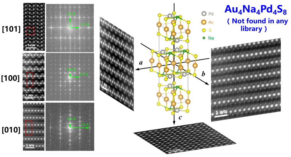
Figure 2. Atomic-scale STEM detailed characterization of quaternary AuPdNaS2 grown on gold foil
Exploring phase transition dynamics in TMC nanowires
Beyond their work in advanced techniques for analyzing complex defect lattice structures, Professor Junhao Lin’s research group studied the atomic-scale phase transition mechanisms of low-dimensional quantum materials through in-situ devices. Transition metal chalcogenide nanowires (TMC-NWs) with an X6Y6 chemical ratio (X=Mo, W; Y=S, Se, Te) represent a metallic phase structure that can be directly transformed from existing low-dimensional transition metal dichalcogenides (TMDs) without the need for additional metal deposition. This makes them potential candidate materials for improving contacts in low-dimensional quantum devices.
To achieve control over the growth orientation of these one-dimensional structures, as shown in Figure 3, they demonstrated a method for guiding the phase transition and growth of highly oriented Mo6Te6 nanowires. They used layered graphite electrodes as a confined encapsulating layer and applied electrothermal stimuli through the graphite electrode to encapsulated two-dimensional MoTe2. Using an in-situ electrothermal MEMS chip platform, they characterized the atomic-scale structural transformation dynamics under in-situ bias voltage conditions. Furthermore, using a similar method, highly oriented nanowires were introduced as lateral contact electrodes in low-dimensional field-effect transistor (FET) devices, achieving a low Schottky barrier of 11.5 meV and an extremely low contact resistance of 43.7 Ω µm at the metal-nanowire interface.
This work demonstrates the direct observation of atomic-scale phase transition dynamics using in-situ techniques. It validates the broad potential of applying this technology to construct high-performance electrical contacts in two-dimensional nano-devices.
The related paper, entitled “Constrained patterning of orientated metal chalcogenide nanowires and their growth mechanism”, has been published in Nature Communications.
Joint doctoral student Qishuo Yang at SUSTech and the University of Queensland is the first author of the paper. Postdoctoral Researcher Liang Zhu from Professor Junhao Lin’s research group (now graduated) and Professor Junhao Lin are the corresponding authors. SUSTech is the first affiliated institution of the paper.
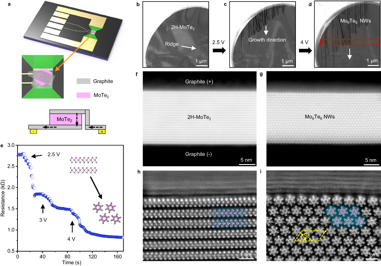
Figure 3. Growth of highly oriented nanowires induced by electrical bias
Innovative phase engineering in quantum devices
In a collaborative effort with a research team from Nanjing University, Professor Junhao Lin’s group has pioneered the use of thermal annealing techniques to activate metal atoms within the metal electrodes of devices, driving their diffusion into the channel material. This work introduced the concept of “on-device phase engineering” for the first time, achieving the in-situ synthesis of various heterojunctions with tunable stoichiometry directly on the chip (Figure 4).
Using the same technique, they further investigated the diffusion process on an in-situ electrothermal MEMS chip platform within STEM, achieving high-precision characterization of the structural transformations in the device electrodes and the resulting phase interfaces. Leveraging this phase transition process, the team characterized the superconductivity exhibited in different phase-transition heterojunctions, observed ultra-low contact resistance formed with p-type semiconductors, and demonstrated exceptional electrocatalytic performance comparable to traditional noble metal catalysts.
The related paper, entitled “On-device phase engineering”, has been published in the prestigious journal Nature Materials.
Doctoral graduate Xiaowei Liu from Nanjing University, Associate Researcher Junjie Shan, doctoral student Tianjun Cao, Postdoctoral Researcher Liang Zhu from Professor Junhao Lin’s research group (now graduated), and doctoral student Jiayu Ma from Sun Yat-sen University are the co-first authors of this paper. The co-corresponding authors include Professor Feng Miao, Associate Professor Shijun Liang from Nanjing University, Professor Xin Luo from Sun Yat-sen University, and Professor Junhao Lin.
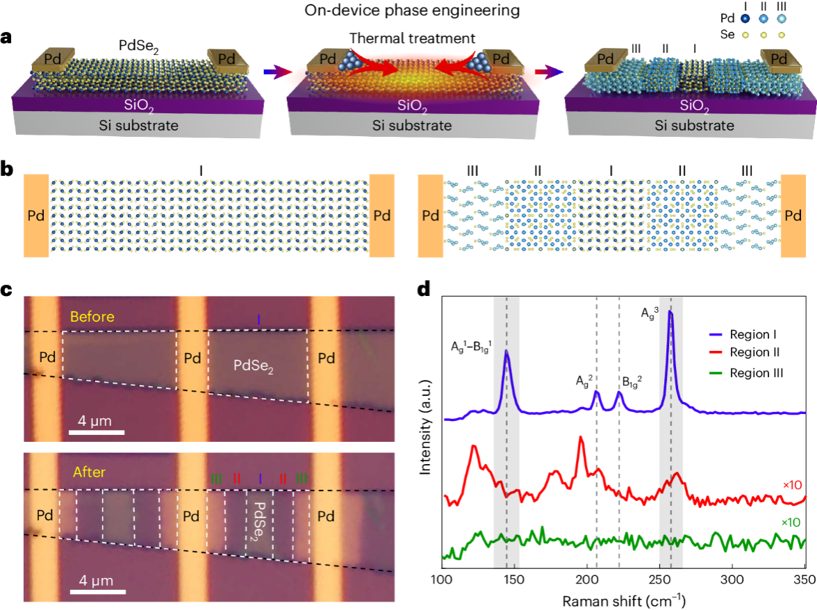
Figure 4. Schematic illustration of the concept of On-device phase engineering
These works were supported by the National Natural Science Foundation of China (NSFC), National Key R&D Program of China, Guangdong Innovative and Entrepreneurial Research Team Program, Science, Technology and Innovation Commission of Shenzhen Municipality, Guangdong Natural Science Foundation, and the Shenzhen Science and Technology Program.
Paper links (In order of appearance above):
Advanced Materials: https://onlinelibrary.wiley.com/doi/abs/10.1002/adma.202402219
Science Bulletin: https://www.sciencedirect.com/science/article/abs/pii/S209592732400505X
Nature Communications: https://www.nature.com/articles/s41467-024-50525-4.pdf
Nature Materials: https://www.nature.com/articles/s41563-024-01888-y
To read all stories about SUSTech science, subscribe to the monthly SUSTech Newsletter.
Proofread ByAdrian Cremin, Yingying XIA
Photo ByDepartment of Physics