Recent emerging applications, such as LiDAR transceivers for autonomous driving and motor drivers for drones and robots, raise the requirements on boost converters (BCs) that can step up voltage from 2.7-4.2V to 12-36V while offering faster transient responses. From the perspective of high voltage conversion ratios (VCRs), capacitor-based converters (CBCs) face challenges of very short turn-on pulses, which limit the switching frequency and increase reliability risks. For transient speed, CBCs inherently suffer from the right-half-plane (RHP) zero. Usually, larger inductors are preferred to reduce ripple, which results in lower-frequency RHP zeros. Recent hybrid BCs primarily adopt switched-capacitor (SC) topology and employ an inductor at the output side to enhance transient response speed. However, the VCR is very limited.
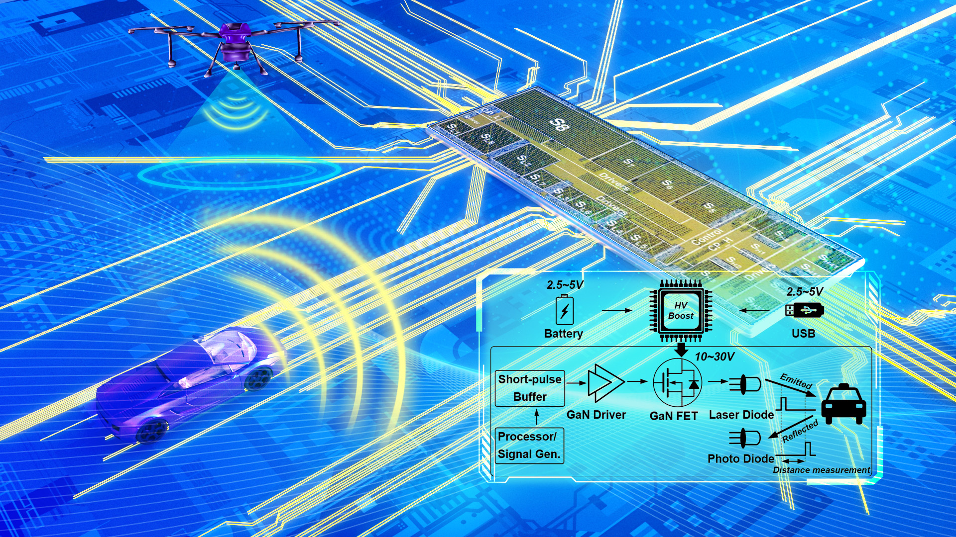
Associate Professor Junmin Jiang’s research group from the Department of Electronic and Electrical Engineering at the Southern University of Science and Technology (SUSTech) has made significant progress in the field of hybrid step-up power converters.
Their paper, titled “A 93%-Peak-Efficiency Battery-Input 12-to-36V-Output Inductor-in-the-Middle Hybrid Boost Converter with Continuous Input and Output Currents and Fast Transient with No RHP Zero”, was presented at the IEEE International Solid-State Circuits Conference (ISSCC), a leading conference in integrated circuit design.
The researchers present a hybrid BC with a small power inductor in the middle of one low-voltage (LV) SC and one high-voltage (HV) SC topology with continuous-input and continuous-output (CICO) current. To achieve a fast response, the 2× SC voltage doubler operates in a two-branch interleaving mode, which provides an output current in a staggered manner while maintaining the 2× conversion ratio. Therefore, the SC doubler can be effectively modeled as an ideal transformer without additional zeros or poles in the overall small-signal transfer function. Such that the CICO boost topology inherently eliminates RHP zeros and possesses the same stability as a buck converter.
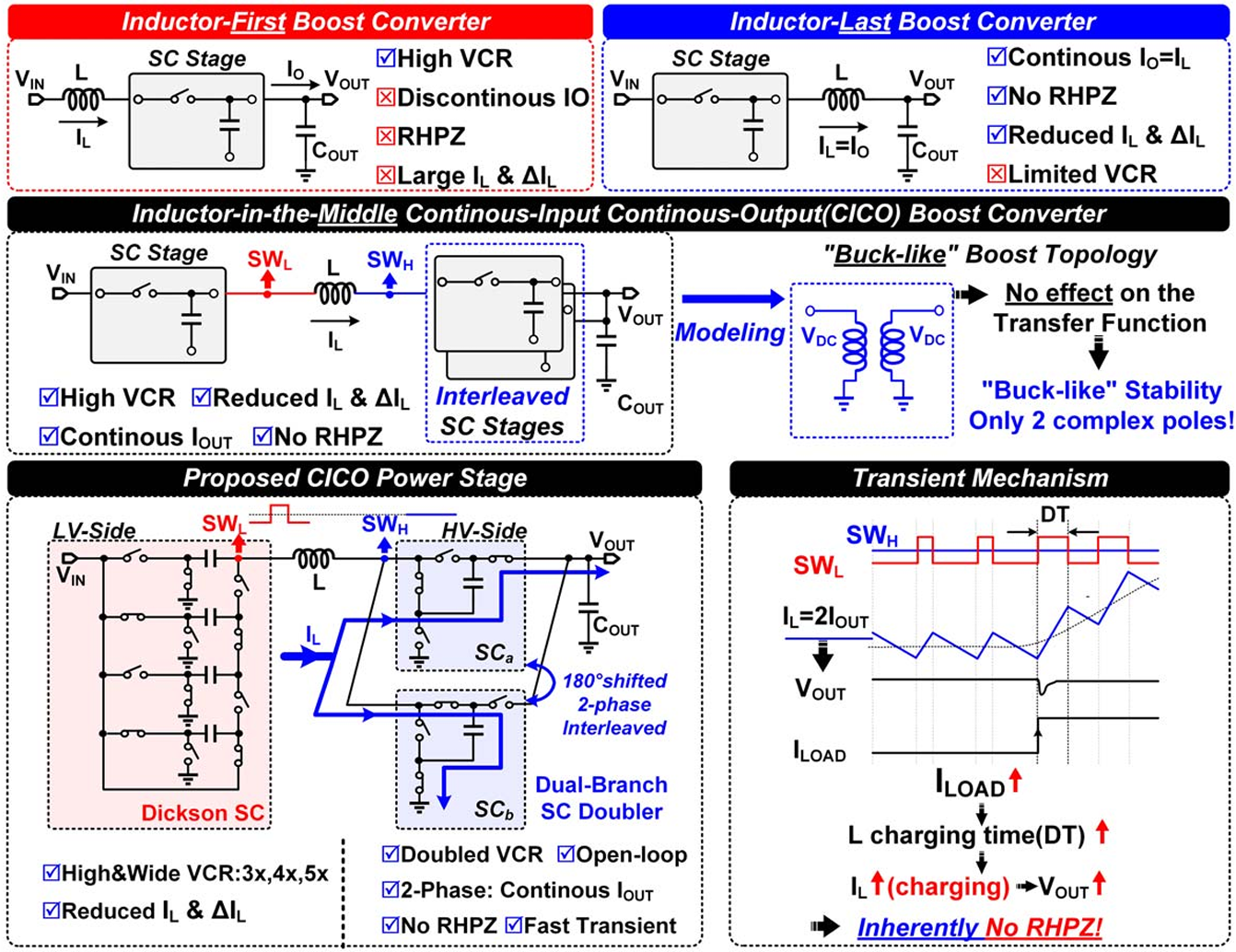
Figure 1. Prior Inductor-First and Inductor-Last topologies and the Inductor-in-the-Middle CICO BC without RHP zeros
The LV SC employs a four-stage Dickson topology with reconfigurable 3×, 4×, and 5× VCRs, and its duty cycle is adjustable (Figure 2). The HV side utilizes a dual-branch interleaving 2× SC doubler and its duty cycle is fixed at 50%. The four branches of the Dickson SC topology allow for reconfiguration by paralleling one or two branches to achieve more VCRs. The inductor voltage and current stress are both released by the HV SC doubler. Therefore, an inductor with low inductance and a compact package can be used, significantly enhancing power density and efficiency.
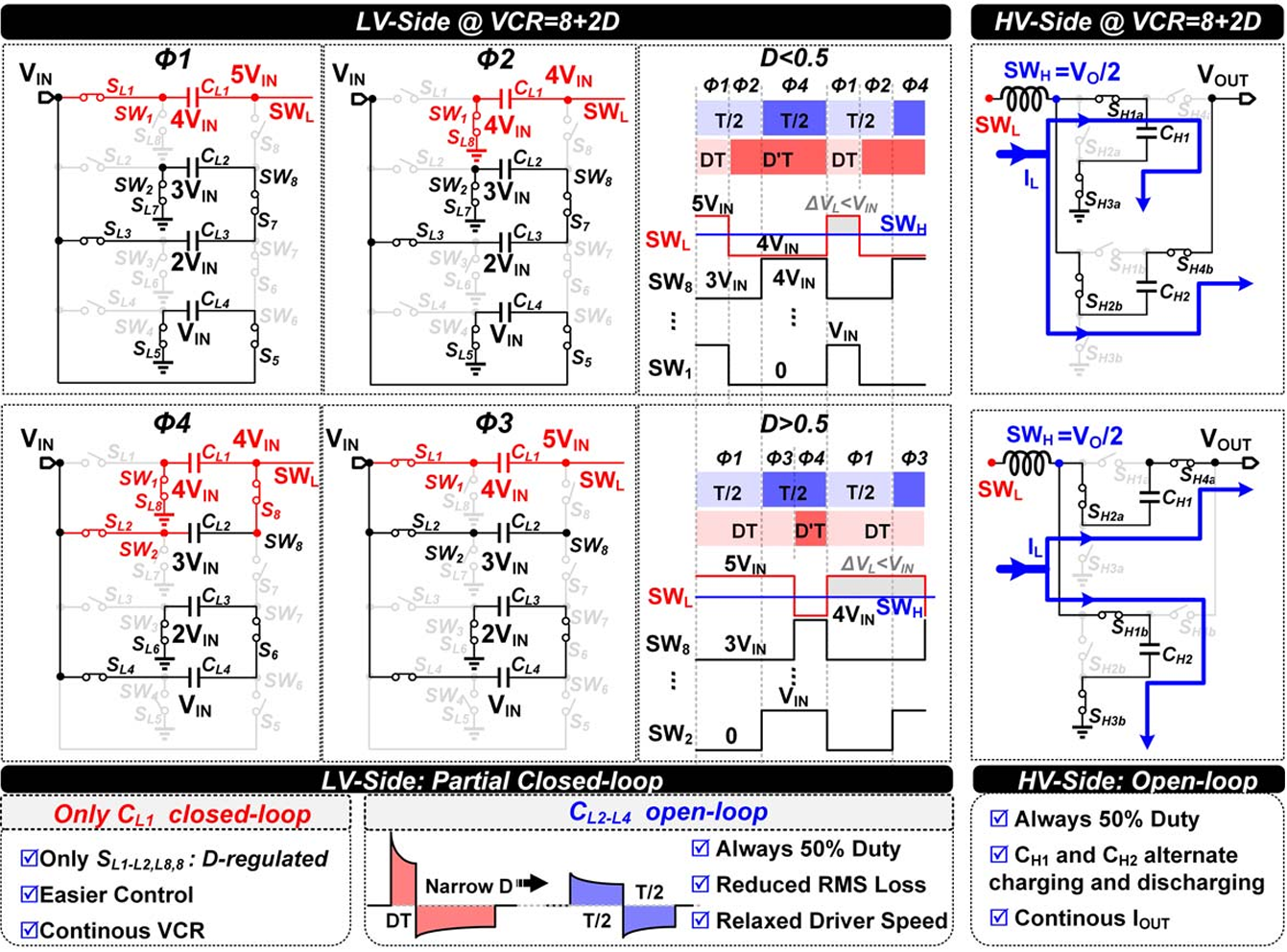
Figure 2. Operating principles of LV-side and HV-side of the CICO BC
The system block diagram includes a Dickson topology on the LV side, where all power switches are 5V transistors, while the remaining switches are LDNMOS transistors with applicable voltage ratings (Figure 3). In terms of control, the feedback loop sampling from VOUT generates a PWM-controlled duty-regulated signal to supply the LV-side switches. All other switches operate in open-loop mode and do not require additional control. In addition, the flying capacitor voltages of the HV-side voltage doubler require voltage calibration to ensure their voltages remain near half VOUT. Ultimately, measurement results verified that under heavy load conditions with VOUT=25V, the flying capacitor voltage calibration improves the efficiency by up to 3% compared to the case without it.
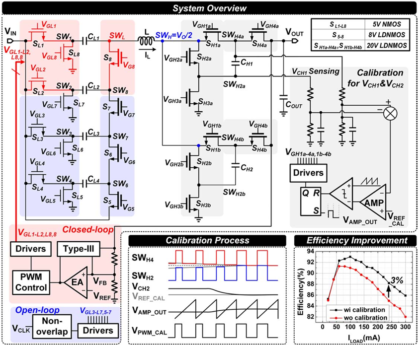
Figure 3. Schematic and calibration process of the CICO BC with measurement results of efficiency improvement by enabling calibration
The CICO converter is fabricated in a 0.18μm BCD process for a 2.7-to-4.2V input and 12-to-36V output DC-DC conversion. The maximum load current is 300mA at 36V, delivering 10.8W maximum output power. When VIN=3.7V and VOUT=30V, a 50ns edge 50-to-300mA load current step results in an overshoot and undershoot as small as approximately 1.7% of the output voltage, which can be negligible, indicating minimal transient effects. With continuous output current and RHP zero elimination, the responding times are 1.4μs and 0.6μs, respectively.
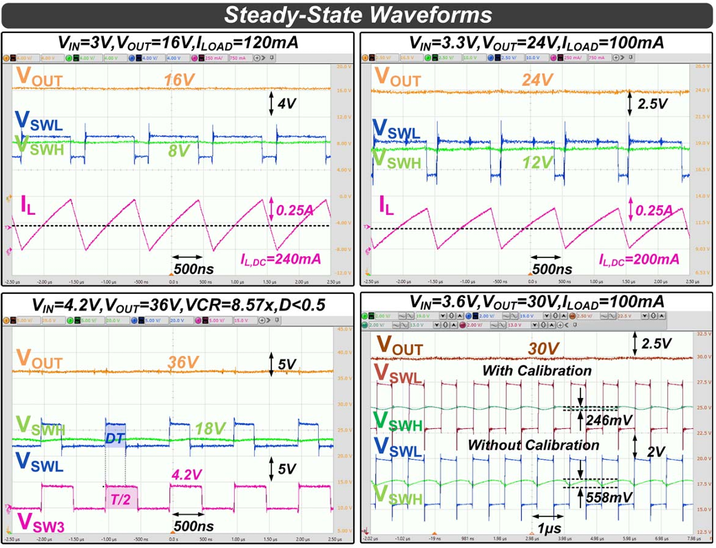
Figure 4. Measured steady-state waveforms of the CICO BC
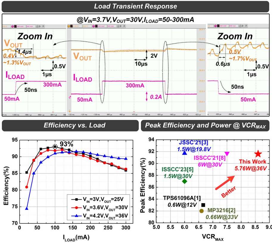
Figure 5. Measured load transient response, efficiency vs. load, and the benchmark with state-of-the-art works
Among the state-of-the-art designs and commercial products listed in the comparison table, the proposed converter achieves a high peak efficiency and the highest power density with a competitive high VCR. The research team reports that this is the first high VCR BC design that maintains a low inductor current while ensuring continuous input and output currents and fast transient response.
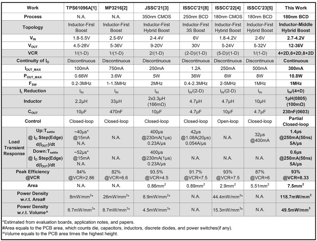
Figure 6. Performance summary and comparison with state-of-the-art
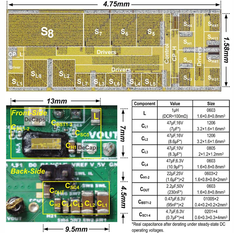
Figure 7. Chip micrograph and photos of the front and back sides of the measurement PCB
Visiting Ph.D. student Yifan Jiang from Junmin Jiang’s research group is the first author of the paper. Associate Professor Junmin Jiang and Professor Yan Lu from Tsinghua University are the co-corresponding authors. SUSTech is the first affiliated institution.
Paper link: https://ieeexplore.ieee.org/document/10904669
To read all stories about SUSTech science, subscribe to the monthly SUSTech Newsletter.
Proofread ByAdrian Cremin, Yuwen ZENG
Photo ByDepartment of Electronic and Electrical Engineering


