Nearly all electronic product systems require a clock, and the clock module is like the “heart” of electronic products. In Internet of Things (IoT) applications, due to the miniaturization of sensor devices, the clock module must develop towards full integration. Since IoT devices are usually powered by low-voltage batteries or the tiny electrical energy collected by energy harvesting modules, the clock module is required to operate with low power consumption. At the same time, the sensor devices of these IoT nodes usually sample at the edges of the clock signal. Therefore, the accuracy and noise of the clock signal are also crucial performance indicators, which determine the speed limit of the entire sampling system.
Although traditional ring oscillators have the advantages of low power consumption and easy integration, their frequency is very sensitive to process, voltage, and temperature (PVT) changes, and additional circuits are needed for compensation. In contrast, relaxation oscillators are easier to integrate on chips and have lower power consumption, making them more suitable for ultra-low-power IoT devices.

A research team led by Associate Professor Junmin Jiang from the Department of Electronic and Electrical Engineering at the Southern University of Science and Technology (SUSTech) has achieved significant progress in low-power and low-noise on-chip oscillators.
Their related achievements, titled “A Dual Slope Boosted Relaxation Oscillator With 2.93 µJ/Cycle Energy Efficiency and 0.068% Period Jitter in 180 nm CMOS”, were published in IEEE Transactions on Circuits and Systems—I: Regular Papers (TCASI), a high-level journal in the field of integrated circuit design.
The research team proposed a 2 MHz relaxation oscillator for low-power IoT node applications. By adopting a cascaded floating inverter amplifier (C-FIA) and dual-slope boosting technology, the jitter of the oscillation frequency was reduced, the power consumption was lowered, and the frequency stability was improved. The oscillator implemented in a 0.18 μm CMOS process achieved an energy efficiency of 2.93 μJ/cycle, a FoMppm of 173 dB, and a FoMpN of 143 dBc/Hz. This oscillator has potential application value in low-power, high-precision IoT and SoC applications (Figure 1).
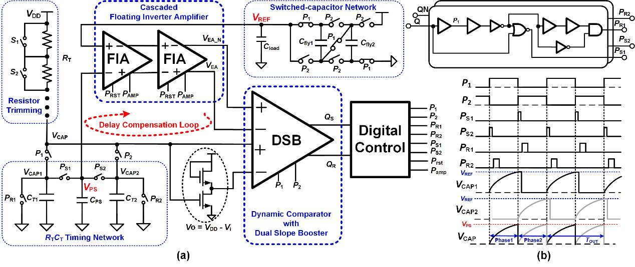
Figure 1. System block diagram of the proposed low-power and low-noise relaxation oscillator
The noise in a relaxation oscillator is mainly caused by the comparison operation when the clock edge is triggered. The jitter is proportional to the input voltage noise of the comparator and inversely proportional to the slope of the RC charging voltage. To reduce the output noise of the oscillator, this work proposed a dynamic comparator with a bidirectional slope compensation module to reduce the output noise of the comparator (Figure 2).
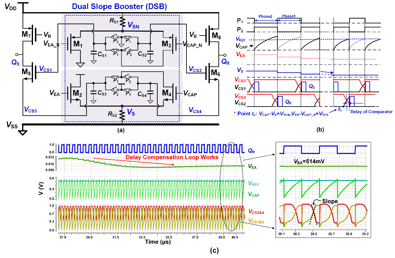
Figure 2. Circuit implementation and waveform diagram of the bidirectional slope-boosted dynamic comparator
To further reduce the power consumption of the system, this team applied the cascaded floating amplifier (C-FIA) in the delay compensation loop. The C-FIA adopted a floating capacitor structure, making its common-mode output voltage unaffected by changes in process, voltage, and temperature (PVT), thus achieving a stable high-gain output (Figure 3). Since the floating capacitor structure does not require a large amount of static current like traditional linear amplifiers, the C-FIA significantly reduces the system’s power consumption while maintaining high gain.
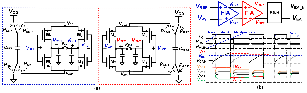
Figure 3. Circuit implementation and waveform diagram of the C-FIA amplifier in the delay compensation loop
The phase noise was measured using a spectrum analyzer (N9020B) (Figure 4), with an average value of -79.78 dB/Hz at an offset of 10 kHz. At the same time, the cycle jitter was measured by a histogram for more than 300,000 consecutive cycles. The average standard deviation of the measured cycle jitter was 345 ps, accounting for only 0.068% of the oscillation period of the output signal.
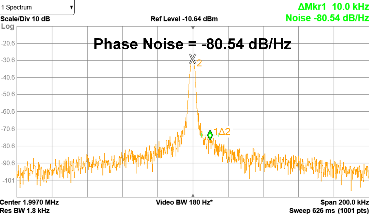
Figure 4. Test results of the phase noise of the output clock
The key performance indicators of the relaxation oscillator were summarized and compared with previous state-of-the-art technologies (Figure 5). In terms of energy efficiency performance, this work ranks second only to the design fabricated using a 28-nanometer process. At the same time, it achieves excellent noise performance, with a value less than half of that of other works. Overall, it achieves excellent jitter performance and good temperature stability at a very low energy consumption. A physical photo of the chip is provided in Figure 6.
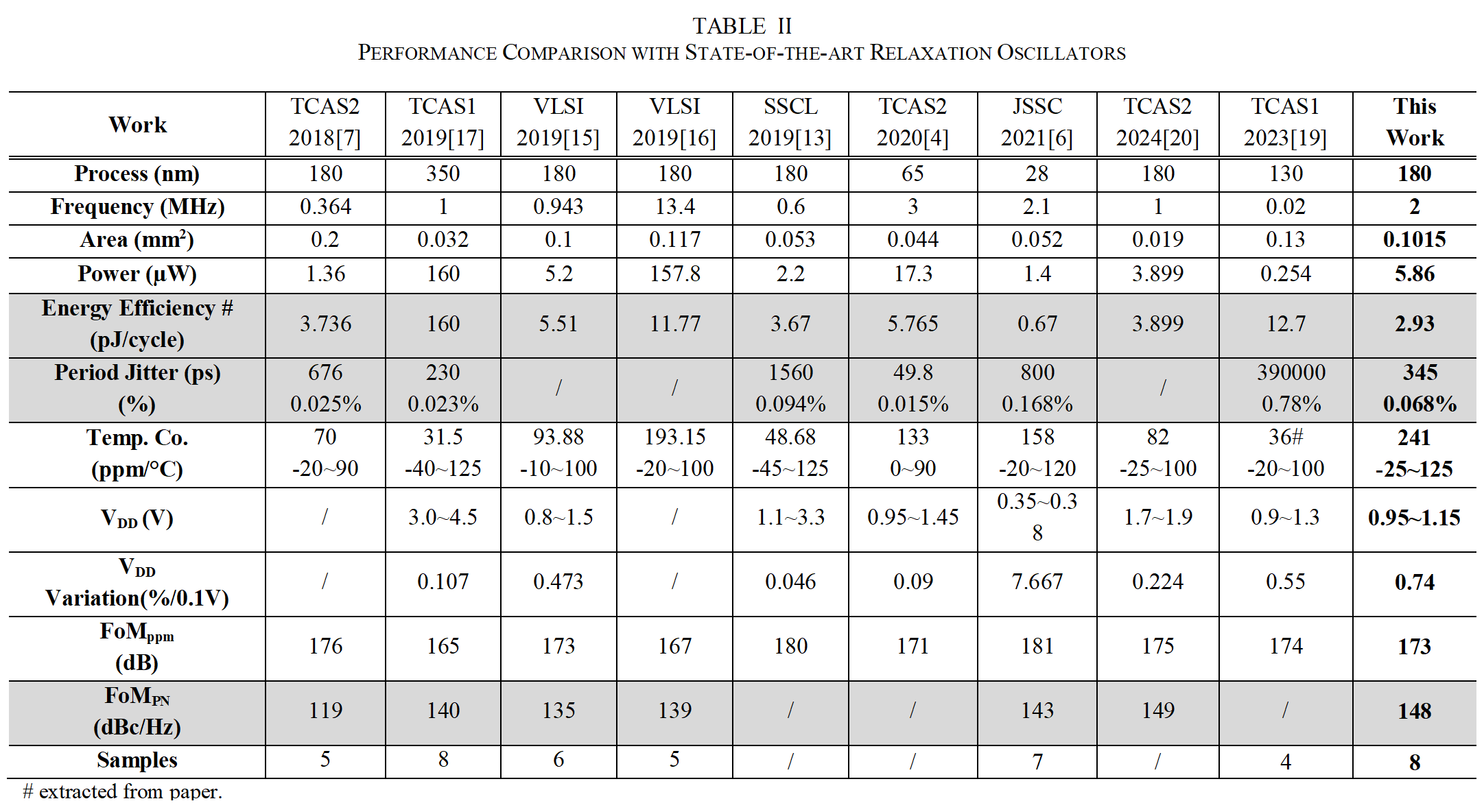
Figure 5. Performance comparison table

Figure 6. Physical photo of the chip
Undergraduate student Yongjuan Shi from the Department of Electronic and Electrical Engineering at SUSTech is the first author of the paper. Associate Professor Junmin Jiang is the corresponding author, with SUSTech serving as the first corresponding institution.
Paper link: https://ieeexplore.ieee.org/stamp/stamp.jsp?tp=&arnumber=10964432
To read all stories about SUSTech science, subscribe to the monthly SUSTech Newsletter.
Proofread ByAdrian Cremin, Yuwen ZENG
Photo ByDepartment of Electronic and Electrical Engineering


