A research team led by Associate Professor Shaolin Xu from the Department of Mechanical and Energy Engineering (MEE) at the Southern University of Science and Technology (SUSTech) has achieved significant progress in ultrafast laser micro/nano manufacturing. Their recent findings have been published in several top-tier journals in manufacturing and optics, including the International Journal of Machine Tools and Manufacture (IJMTM), the International Journal of Extreme Manufacturing (IJEM), Laser & Photonics Reviews (LPR), Advanced Functional Materials (AFM), and Advanced Material Technologies (AMT).
Revolutionary laser precision micromachining of single-crystal silicon carbide
Microgrooves with diverse cross-sections are required in various fields but remain a significant challenge in precision machining, especially for hard-to-machine materials. Patterned laser ablation offers an avenue for fabricating microgrooves on any material with notably enhanced shape diversity.
However, it is hard to precisely control the groove’s cross-sectional profiles due to the complex ablation process, including the diffraction-induced energy distribution variations away from the focal plane and the inconsistent polarization-related energy absorption. These factors complicate the relationship between beam spot shape and ablated groove shape, making it challenging to design appropriate spot shapes for specific groove requirements.
The team developed an adaptive beam-shaping method for laser spot design to improve microgrooves’ shape accuracy (Figure 1). Combining laser diffraction and polarization effects, they established a profile evolution model of the laser ablation to accurately predict groove shapes, guiding the iterative beam-shaping procedure. The beam spot shape is iteratively fine-tuned until the deviation between the simulated and the target groove’s profile meets the accuracy requirements.
Using this approach, they decreased the root mean square error of the groove profile to less than 0.5 μm when processing microgrooves with a width of 10 μm (Figure 2). Various microgrooves with precise cross-sections, including triangles, trapezoids, and functionally contoured microstructures, were achieved by patterned laser direct writing assisted with the adaptive beam-shaping method. This strategy paves the way for laser ablation of microgrooves with high shape accuracy for traditional hard-to-machine materials.
This work, entitled “Adaptive beam-shaping enabled high-precision patterned laser micro-grooving,” has been published in the International Journal of Extreme Manufacturing.
Dr. Pei Qiu and Ph.D. candidate Jun Li from the Department of MEE at SUSTech are the co-first authors of the paper. Associate Professor Shaolin Xu is the corresponding author, and SUSTech is the primary affiliated institution. Other contributors to this study include Dandan Yuan, Zixuan Xin, and Jiaxu Huang from Shaolin Xu’s team.
Figure 1. Flow diagram of the adaptive beam-shaping method based on an accurate evolution model.
Figure 2. Validation of shape control capability and deviation analysis for diverse cross-sectional profiles. (a) Triangle; (b) Trapezoidal; (c) Semicircular; (d) U-shaped.
Breakthrough in innovative all-glass nanohole metalens design and ultrafast laser fabrication technology
Metalenses are lens devices composed of subwavelength structural units, capable of efficiently manipulating light fields by precisely controlling the phase, amplitude, and polarization of light waves. Compared to traditional optical devices, metasurfaces offer advantages such as thinness, compactness, and multifunctional integration, demonstrating significant potential in imaging, display, sensing, and communication applications. However, traditional nanopillar-based metalenses often face challenges of insufficient phase delay due to the limited aspect ratio and duty cycle of their structural units, which restricts their performance and application scope.
To address this challenge, the researchers introduced a novel design and ultrafast laser fabrication method for all-glass nanohole metalenses. By utilizing high-aspect-ratio nanoholes with subwavelength periods, tunable depths, and fixed duty cycles as phase-shifting units, an ideal linear 2π phase delay was achieved, enabling excellent light modulation performance (Figure 3).
They developed a non-diffracting laser lithography technique, employing a unique Bessel beam modulated by a concave-axicon phase diagram to ensure consistent hole diameter along the depth. Combined with post-processing techniques, the method produced damage-free nanohole arrays with periods as small as 800 nm and precisely controlled depths exceeding 10 μm. This technology enables the rapid production of high-performance all-glass nanohole metalenses with a modulation efficiency of up to 97% at a wavelength of 1.55 μm.
Additionally, the study demonstrated the fabrication of a large 2-cm-diameter metalens, along with various optical devices such as axicons, vortex waveplates, and blazed gratings (Figure 4). This research opens a new avenue for all-glass metalenses, making customized metalenses more economical and accessible.
The work, titled “All-glass Nanohole Metalens by Non-diffracting Laser Lithography,” was published in Laser & Photonics Reviews.
Postdoctoral researcher Kang Xu and Mandong Zheng from the Department of MEE at SUSTech are the co-first authors of the paper. Associate Professor Shaolin Xu is the corresponding author, and SUSTech is the is the primary affiliated institution.
Figure 3. Schematic of ultrafast laser fabrication for all-glass nanohole metalenses.
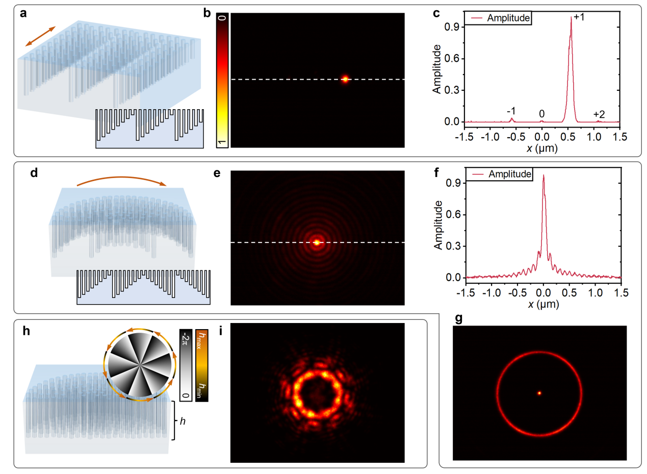
Figure 4. Diverse metalens devices. (a-c) Blazed grating; (d-g) Large base-angle (17°) axicon; (h-i) Eight-order vortex waveplate.
Laser-based fabrication of anti-reflective optical elements with high damage threshold
Anti-reflective optical components play a critical role in modern optical applications, particularly in laser processing systems. Yet, conventional coating-based anti-reflective methods face challenges under high-power laser irradiation, limiting their broader application. Enhancing the laser-induced damage threshold (LIDT) of anti-reflective technology to meet high-power laser demands remains an urgent research priority.
To address this, the research team proposed an ultrafast laser processing technique combined with an in-situ dewetting-assisted plasma etching (in-situ DAPE) method (Figure 5). By depositing a platinum (Pt) metal film on fused silica substrates, uniform nanoscale metal particles were formed under sustained high-energy plasma irradiation and bombardment via Rayleigh instability. These nanoparticles acted as etching masks, enabling the fabrication of densely arranged conical nanostructures on the substrate.
Through this process, they achieved high-efficiency preparation of hybrid anti-reflective structures comprising optical microstructures and nanocone arrays on fused silica surfaces. The formation of nanocones relied on the Marangoni effect-driven dewetting behavior of the Pt film under plasma beam irradiation, which generated uniform, etch-resistant nanoparticle masks. By adjusting the metal film thickness or incorporating passivation-assisted secondary etching, nanocone arrays with tunable diameters (62-136 nm) and heights (126-942 nm) were flexibly fabricated.
The resulting anti-reflective micro-optical components exhibited an average transmittance of 98% across the 0.3-2.5 μm wavelength range, a 1.1-fold improvement in focusing efficiency, and retained 79.4% of the original LIDT of fused silica (Figure 6), demonstrating high laser damage resistance.
This study, titled “In Situ Dewetting Assisted Plasma Etching of Large-Scale Uniform Nanocones on Arbitrarily Structured Glass Elements,” was published in Advanced Functional Materials.
Ph.D. candidate Jin Hu from the Department of MEE at SUSTech is the first author of the paper. Associate Professor Shaolin Xu is the corresponding author, and SUSTech is the primary affiliated institution.
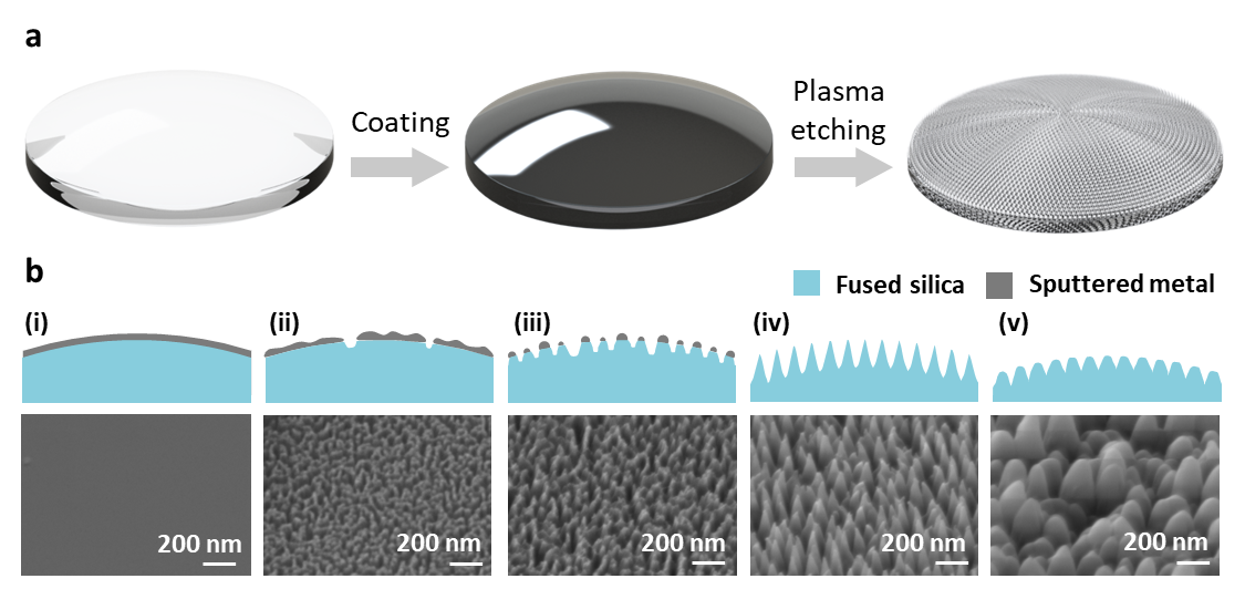
Figure 5. Illustration of proposed one-step in situ DAPE method for fabrication of engraved nanocones.
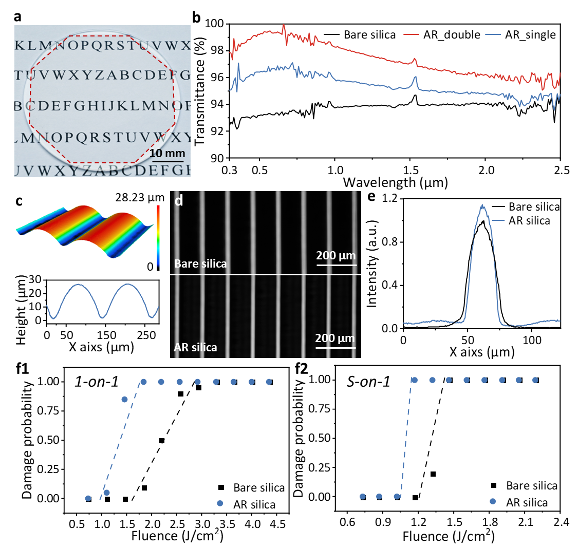
Figure 6. The optical performances of silica wafers and micro-cylindrical lens arrays with or without engraved nanocones.
Patterned laser lithography enables scalable fabrication of MIM metasurfaces
Metal-insulator-metal (MIM) metasurfaces are promising optical devices for beam shaping, holography, and infrared absorption, which offer low loss, high modulation efficiency, and compatibility with various fabrication techniques. However, traditional fabrication methods often struggle to simultaneously achieve high resolution and large-area consistency, limiting the scalability of MIM devices in practical applications.
The researchers proposed a novel technique called Cross-Scale Patterned Pulse Laser Lithography (PPLL). This method utilizes a spatial light modulator (SLM) to shape ultrafast laser beams into binary patterns, enabling the direct fabrication of complex freeform structures in a single laser exposure. An optimized 8f optical system and grayscale anti-Gaussian mask were used to ensure uniform energy distribution. The technique enables single-shot exposure areas exceeding 100*100 μm2, with a spatial resolution approaching the diffraction limit (~300 nm), thus balancing high precision with large-area consistency.
In terms of device architecture, they developed an MIM structure composed of a 20 nm Ge2Sb2Te5 (GST) top layer, an Al2O3 dielectric interlayer, and a metallic reflective bottom layer. Both simulation and experimental results confirm that this multilayer configuration supports a near half-wave phase delay, effectively overcoming the phase modulation limitations of ultrathin single-layer films and significantly enhancing light field control capabilities (Figure 7).
Based on this technique, the research team successfully fabricated highly uniform and efficient Dammann gratings, as well as MIM holographic devices capable of producing clearly reconstructed images. The method enables centimeter-scale devices to be manufactured within minutes, demonstrating exceptional fabrication efficiency and optical modulation performance (Figure 8).
This work provides a new route for the scalable fabrication of MIM metasurfaces using ultrafast laser technology and opens up novel possibilities for the development of high-performance, low-loss planar photonic devices.
The study, titled “Cross-Scale Patterned Pulse Laser Lithography for MIM Meta-Devices Processing,” was published in Advanced Materials Technologies.
Ph.D. candidate Lingyu Huang from the Department of MEE at SUSTech is the first author of the paper. Associate Professor Shaolin Xu is the corresponding author, and SUSTech is the primary affiliated institution.
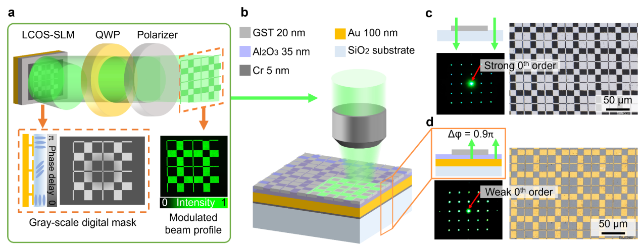
Figure 7. Schematic of the cross-scale patterned pulse laser lithography method.
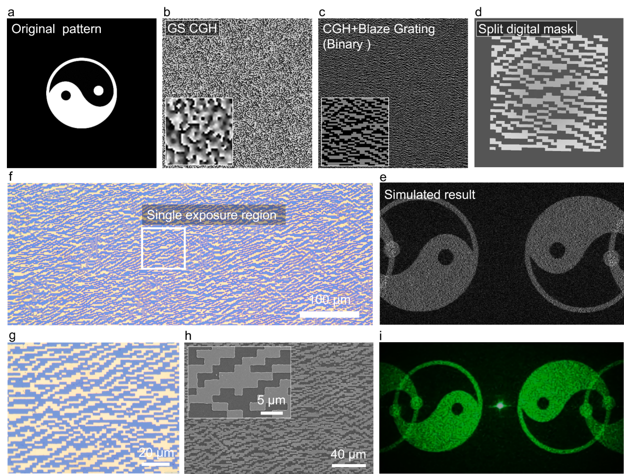
Figure 8. Design and characterization of the MIM holographic metasurface.
Atomic-level insights into phase transition mechanism in femtosecond laser processing of diamond
Diamond is an exceptionally wide-bandgap semiconductor, ideal for applications in electronics and quantum technologies. While femtosecond laser processing enables micro/nano fabrication of diamond, the dynamic atomic-level structural evolution during this process remains poorly understood, limiting the further development of this technique in cutting-edge applications.
In this study, the researchers propose that repeated exposure to femtosecond laser pulses induces cycles of ultrafast lattice heating on the diamond surface. The irreversible structural changes caused by early pulses fundamentally alter the material’s current state, thereby influencing subsequent laser–material interactions and driving the sequential evolution of surface and subsurface structures.
Through a comprehensive investigation of the dynamic structural evolution in diamond during femtosecond laser multi-pulse processing—taking into account ultrafast dynamics, electric field distribution, and ablation phenomena—they introduce a sequential evolution pathway for nanocomposite carbon structures. The study further reinterprets the initiation, transformation, and stabilization processes that were previously broadly categorized as “graphitization” (Figure 9). Specifically, the evolution from diaphite to diamond-OLC (onion-like carbon) and the transition from amorphous carbon to planar-oriented graphite are reported under femtosecond laser surface processing.
This research provides atomic-scale insights into diamond’s response in femtosecond laser processing, offering a theoretical foundation for ultra-precision micro/nano fabrication of diamond and the development of functional carbon materials.
This work was published in the International Journal of Machine Tools and Manufacture under the title “Atomic-level insight into sequential evolution of nanocomposite carbon structures in femtosecond laser processing of diamond.”
Dr. Huili Han is the first author of the paper. Associate Professor Shaolin Xu and Chair Professor Bi Zhang are the co-corresponding authors, and SUSTech is the primary affiliated institution.
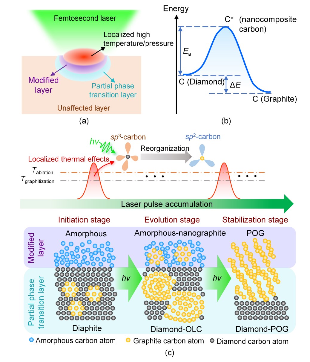
Figure 9. Schematic diagram of femtosecond laser-induced phase transition mechanisms in diamond.
Systematic review of super-resolution laser machining
Super-resolution laser machining breaks the optical diffraction limit, enabling high-precision micro/nano fabrication in semiconductors, biomedicine, and nanotechnology. Despite its promise, conventional laser technology faces a resolution-efficiency trade-off: achieving high precision typically requires excessive energy consumption and low throughput, while large-scale production requires compromised accuracy, limiting industrial applications.
This review systematically analyzes two core approaches (Figures 10 and 11). The first, “reducing the diffraction limit,” involves compressing spot size via shorter wavelengths and optimized focusing systems. The second, “surpassing the diffraction limit,” relies on overcoming optical constraints through nonlinear effects, near-field enhancement, and other phenomena.
By tailoring laser parameters, optimizing processing strategies, applying spatiotemporal modulation to control light-matter interactions, and developing high-speed optical machining systems, researchers can significantly mitigate the resolution-efficiency trade-off. The review further highlights future directions and industrial potential through interdisciplinary integration, providing a critical theoretical framework for next-generation precision manufacturing.
This review, titled “Super-resolution laser machining,” was published in the International Journal of Machine Tools and Manufacture.
Dr. Jiaxu Huang is the first author. Associate Professor Shaolin Xu is the corresponding author, and SUSTech is the primary affiliated institution. Postdoctoral researcher Kang Xu also contributed to this work.
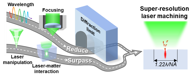
Figure 10. How to achieve super-resolution laser machining
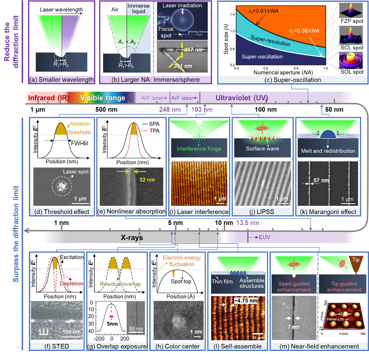
Figure 11. Two approaches for super-resolution laser machining
Paper links (In order of appearance above):
IJEM: https://iopscience.iop.org/article/10.1088/2631-7990/adec26
LPR: https://onlinelibrary.wiley.com/doi/10.1002/lpor.202402006
AFM: https://advanced.onlinelibrary.wiley.com/doi/10.1002/adfm.202410563
AMT: https://advanced.onlinelibrary.wiley.com/doi/10.1002/admt.202500131
IJMTM: https://linkinghub.elsevier.com/retrieve/pii/S0890695525000021
IJMTM: https://www.sciencedirect.com/science/article/pii/S089069552500001X?via%3Dihub
To read all stories about SUSTech science, subscribe to the monthly SUSTech Newsletter.
Proofread ByAdrian Cremin, Yuwen ZENG
Photo ByDepartment of Mechanical and Energy Engineering


