At the end of November, Southern University of Science and Technology (SUSTech) had the research group led by Department of Physics Associate Professor Liyuan Zhang make important breakthroughs in wide spectral photodetectors based on 2D materials. Research Associate Professor Youpin Gong worked in collaboration with Associate Professor Rui Chen from the Department of Electrical and Electronic Engineering.
The paper titled “Ultrahigh-Sensitive Broadband Photodetectors Based on Dielectric Shielded MoTe2/Graphene/SnS2 p-g-n Junctions” was published in the top journal Advanced Materials (impact factor, 21.950). The first and second authors are doctoral candidate Alei Li and class of 2016 undergraduate Qianxue Chen respectively, who both study in his Mesoscopic Physics Lab of SUSTech. Research Associate Professor Youpin Gong from the SUSTech Academy for Advanced Interdisciplinary Studies is the corresponding author, Department of Physics Associate Professor Liyuan Zhang and Department of Electrical and Electronic Engineering Associate Professor Rui Chen are the co-corresponding authors. Judy Z. Wu, a distinguished professor of the Department of Physics and Astronomy at the University of Kansas, also significantly contributed to the research work.
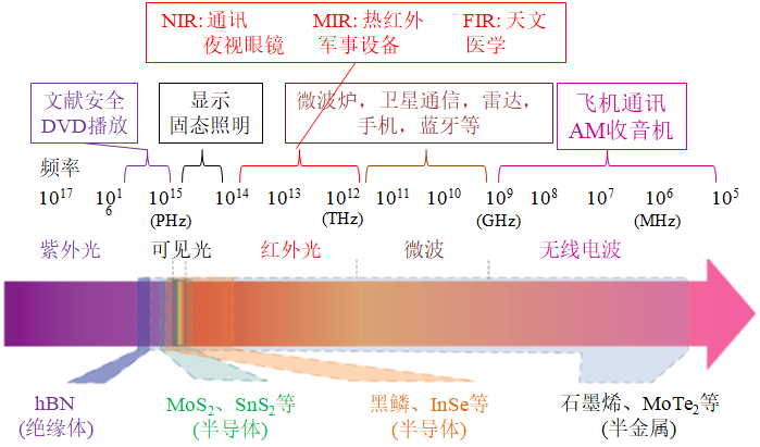
Photodetectors capable of detecting light in a wide spectrum is central to diversified optoelectronic applications in spectroscopy, remote sensing, imaging, and optical communication. At present, Si-based and InGaAs photodetectors are widely used in life. However, the Si-based photodetector can only detect a narrow spectral range (200−1100 nm). For InGaAs photodetectors, its raw materials are toxic and expensive, and the requirement to operate in a low-temperature environment (~4 K) makes it costly to use. With the development of technology and market, the demand for high-sensitivity, high-speed, broadband, low-cost, flexible photodetectors is increasing, so traditional semiconductor photodetectors are increasingly unable to meet future technological needs. Two-dimensional (2D) materials are available in a wide range of applications for photodetection from the ultraviolet to the radio range depending on different bandgaps and doping due to their rich variety (Figure 1, Nature Photonics 2014, 8, 899). Especially with the characteristics of miniaturization, portability, and flexibility, it is expected to become a huge potential for next-generation optoelectronic devices.
However, a single 2D material photodetector has the disadvantages of narrow detection bands, long response times, or low detection rates. To improve the performance of 2D material photodetectors, the researchers proposed to use a new structure: 2D van der Waals (vdW) p−n heterojunction. This photodetector is mainly based on the photovoltaic effect of the p−n junction. Its main defects or challenges are: although these photodetectors exhibit a promising detectivity because the built-in electric field can efficiently inhibit the noise derived from the random carriers’ transport, the photoresponsivity is fairly low (0.01−1.0 A/W in the near infrared) due to the lack of internal gain. In addition, most of the reported vdW p–n junction devices are narrowband operating primarily in the visible spectrum only. It is therefore important to realize both high detectivity by increasing the photoresponsivity and broadband through the design of vdW p–n junctions with photoactive 2D layers beyond the visible spectrum.

Figure 1. Applicable spectral range of various 2D material photodetectors
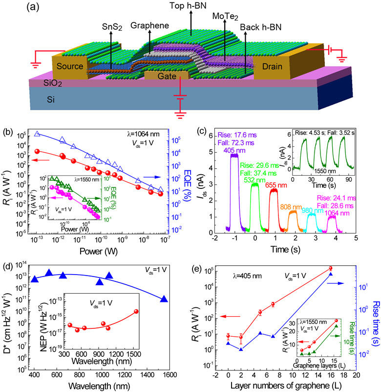
To overcome this challenge, under the direct guidance of Associate Professor Youpin Gong and after experiencing a large amount of experimental accumulation for more than one year, the research team member Alei Li and physics undergraduate Qianxue Chen designed a novel 2D h-BN/MoTe2/graphene/SnS2/h-BN vdW p–g–n junction, introducing a graphene interlayer and h-BN dielectric shielding layer and realized both high detectivity and responsivity in a wide spectral range (405−1550 nm) (Figure 2).
The combination of the MoTe2 and SnS2 of complementary bandgaps and the graphene interlayer provides a unique vdW heterostructure with a vertical built-in electric field for high-efficiency broadband light absorption, exciton dissociation, and carrier transfer. The graphene interlayer plays a critical role in enhancing sensitivity and broadening the spectral range (Figure 2e). An optimized device containing 5−7-layer graphene has been achieved and shows an extraordinary responsivity exceeding 2600 A/W with fast photoresponse and specific detectivity up to ~1013Jones in the ultraviolet−visible−near-infrared spectrum (Figure 2b−d). Especially, the detectivity up to 1.06×10¹¹ Jones under 1550 nm short-wave infrared (SWIR) excitation at room temperature is even comparable with commercial SWIR photodetectors such as uncooled Ge-on-Si photodetectors. This result provides a viable approach to future ultrahigh-sensitivity and broadband photonic detectors.

Figure 2. Device structure and photodetection performance. (a) 3D diagram of the device structure. (b) Photoresponsivity and external quantum efficiency. (c) Photoresponse speed. (d) Detectivity and noise equivalent power. (e) The effect of graphene interlayer thickness on the responsivity and response speed.
This work is supported by many foundations including the start-up funds of SUSTech, the Shenzhen Municipal Science and Technology Innovation Commission, National Natural Science Foundation of China, and the Guangdong Innovative and Entrepreneurial Research Team Program.
Article link: https://onlinelibrary.wiley.com/doi/abs/10.1002/adma.201805656
Proofread ByXia Yingying
Photo ByDepartment of Physics