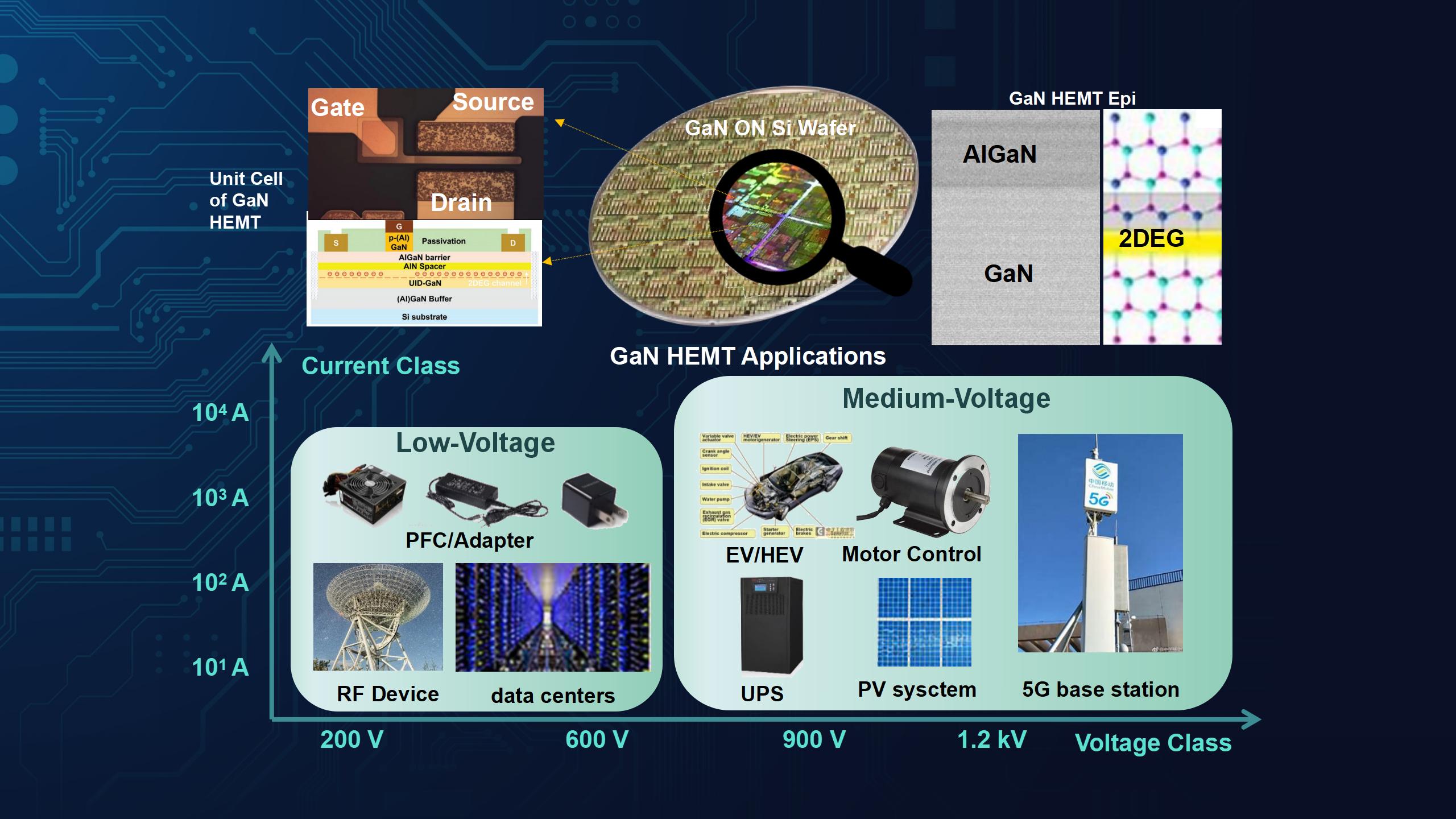
Gallium nitride (GaN), as the representative material of the third generation of semiconductors, has the advantages of a large band gap, high critical breakdown field strength, high electron mobility, and high operating temperature. GaN-based field-effect transistors have received extensive attention in research and industry due to their excellent characteristics such as low on-resistance, high power, high frequency, high efficiency, and light weight. The high efficiency power supply of GaN technology plays a significant role in the green energy of solar and wind, automotive electric, rail traffic, machine tools, medical equipment, high-speed switch, wireless power, and white household appliances.

Professor Hongyu Yu’s research group from the School of Microelectronics (SME) at the Southern University of Science and Technology (SUSTech) has recently achieved a series of important developments in the field of GaN devices.
These research results have been published in high-ranking international journals in the areas of microelectronic devices, including IEEE Electron Device Letters (IEEE EDL), Applied Physics Letters, and IEEE Transactions on Electron Devices (IEEE TED).
Etching-free normally-off GaN recessed-gate MIS-HEMT
For energy saving and safety considerations, the normally-off operation of GaN HEMT is necessary to simplify the circuit design and build a fail-safe system. For the first time, Prof. Yu’s research group developed two regrowth processes that yield a series of etching-free normally-off AlGaN/GaN recessed-gate MIS-HEMTs. Generally, an etching process is required to define the gate region in GaN recessed-gate HEMT, which would introduce plasma damage and surface defect. The regrowth technique can effectively alleviate the etching damage, while the optimized nitride passivation is difficult to be applied during this recess-first process.
This work was applied in-situ SiNx passivation in regrowth processes and achieved a high threshold voltage (Vth > 2.5 V) with world-record low on-state resistance and Vth hysteresis. The in-situ SiNx with regrowth technique shows great potential in achieving high-performance GaN normally-off MIS-HEMTs.
The study, entitled “Normally-OFF AlGaN/GaN MIS-HEMTs With Low RON and Vth Hysteresis by Functioning In-Situ SiNx in Regrowth Process,” was published in IEEE EDL.
Jiaqi He, a joint Ph.D. student of the School of Microelectronics (SME) at SUSTech and Hong Kong Polytechnic University (PolyU), is the first author of this paper. Prof. Hongyu Yu is the corresponding author, and SUSTech is the first affiliated unit. This work was also supported by Prof. Gang Li from PolyU.

Figure 1. (A) Device structure of GaN MIS-HEMT; (B) AFM/TEM results of regrowth structure; (C) Transfer/Output characteristic of normally-off devices; (D) Benchmark of Device Vth-Ron.
p-GaN Gate Normally-off HEMTs
The gate breakdown voltage and reliability of power-switching devices play an important role in industrial production and practical applications. Typically, p-GaN gate normally-off HEMTs are used as switches in high-power supply circuits. However, there are still some problems in this already commercialized device structure: the gate breakdown voltage is low, and the device is not reliable enough for a long time under the high gate drive voltage.
In order to solve the above problems, Prof. Yu’s team effectively reduced the peak electric field of the gate metal/p-GaN Schottky junction by regulating the parameters of p-GaN in the epitaxial growth process. Without affecting properties such as threshold voltage, on resistance, and other DC characteristics, the team prepared a normally-off HEMT with 10-year operating reliability under 10.6 V gate drive voltage. The u-GaN/p-GaN structure proposed in this study can effectively improve the reliability of the power conversion system.
This work, entitled “p-GaN Gate HEMTs With 10.6 V Maximum Gate Drive Voltages by Mg Doping Engineering,” was published in IEEE TED.
Guangnan Zhou, a joint Ph.D. student at SUSTech and the University of British Columbia (UBC), is the first author of this paper. Prof. Hongyu Yu is the corresponding author. This work was also supported by Prof. Guangrui Xia at UBC.

Figure 2. (A) Device cross-section diagram and AFM results; (B) Weibull diagram and device life prediction; (C) at Gate breakdown characteristics of devices (a) at 25℃, (b) at 150℃; (D) Benchmark of VG-max and VTH.
Gold-free ohmic contact on InAlN/GaN heterostructures
GaN HEMT device based on InAlN/GaN heterostructures is a promising candidate for realizing the next generation low switching-loss, high power density, and high switching speed electronic devices due to its high two-dimensional electron gas density and lower sheet resistance. Lowering the source/drain contact resistance (Rc) is critical for obtaining a high-performance InAlN/GaN-based HEMT device.
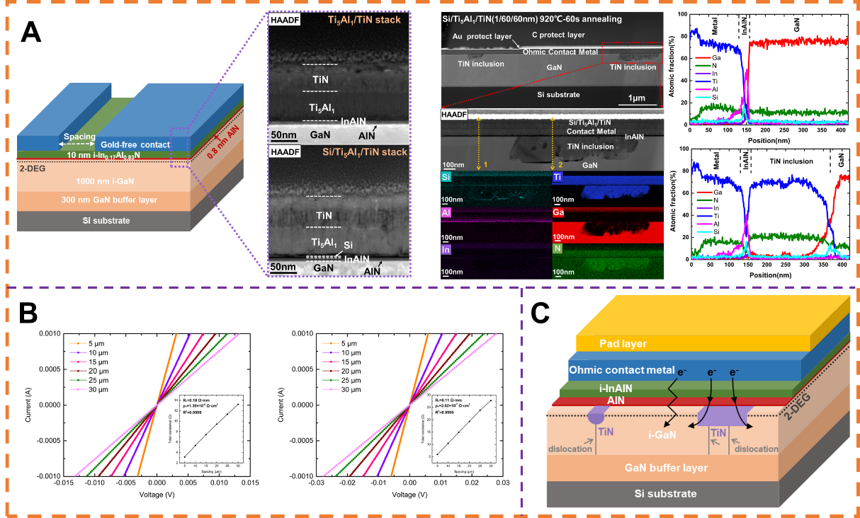
Prof. Yu’s team utilized Si/Tl5Al1/TiN as a source/drain ohmic contact stack for i-InAlN/GaN heterostructures (Figure 3A). Compared with the conventional gold-based metal stacks, the proposed structure is compatible with the current Si-COMS process line and is more cost-efficient. An ultra-low contact resistance of 0.11 Ω·mm (ρc = 2.62×10⁻⁷ Ω·cm2) was obtained after 950℃ annealing, which is comparable to the best-reported results of regrowth and barrier recess technologies (Figure 3B). Moreover, the mechanism of this ohmic contact structure was fully understood through microscopic and thermodynamic analyses, and the simultaneous effects of tunneling and spike mechanism were proved (Figure 3C). These results shed light on the mechanism for the formation of ohmic contact in a gold-free metal stack for GaN-based HEMTs.
This work, entitled “Microscopic formation mechanism of Si/Ti5Al1/TiN ohmic contact on non-recessed i-InAlN/GaN heterostructures with ultra-low resistance”, was published in Applied Physics Letters.
Yang Jiang, a visiting Ph.D. student of SME at SUSTech, is the first author of this paper. Prof. Hongyu Yu and Research Assoc. Prof. Qing Wang are the co-corresponding authors. SUSTech is the first affiliated unit.

Figure 3. Gold-free ohmic contact on InAlN/GaN heterostructures. (A) Schematic cross-sectional of Ti5Al1/TiN and Si/Ti5Al1/TiN ohmic contact and STEM images; (B) I–V characteristics of CTLM and linear fitting of the total resistance vs. spacing; (C) Schematic of the proposed simultaneous effects of tunneling and the spike mechanism.
P-type ohmic contacts on double-channel heterostructures
The development of high-performance GaN p-FETs has become the primary problem in achieving high-performance GaN CMOS. The ohmic contact of the source/drain terminal is the basis for the connection between the device and the external circuit. Its performance is closely related to the device output current, knee point voltage, conduction resistance, power loss, and reliability. Therefore, the development of low-resistance ohmic contact is the key to improving the performance of GaN p-FETs.
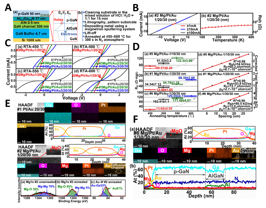
Prof. Yu’s team developed a p-type ohmic contact on GaN CMOS epitaxy by using Mg/Pt/Au metal stack. The achieved specific contact resistance reached a record low value of 1.810-5Ω2. In addition, the technology of in-situ removal of GaOx on the p-GaN surface was demonstrated, which improved the device reliability induced by conventional surface treatment technology.
The outcomes show that the Mg contact layer promotes the Pt layer to form an Au diffusion channel, which drives the inward diffusion of Au to contact p-GaN. At the same time, Au at the interface induces the outward diffusion of Ga to form an Au-Ga phase, and forms Ga vacancies on the p-GaN surface to increase the hole concentration. These results explain the mechanism for forming the ultra-low ohmic contact resistance.
This study, entitled “Ohmic Contact with a Contact Resistance of 12 Ω·mm on p-GaN/AlGaN/GaN,” was published in IEEE EDL.
Chuying Tang, a joint doctoral candidate SUSTech and the Harbin Institute of Technology (HIT), is the first author of this paper. Prof. Hongyu Yu and Assoc. Prof. Qing Wang are the corresponding authors. This work was also supported by Prof. Yulong Jiang from Fudan University. SUSTech is the first affiliated unit.

Figure 4. (A) Epitaxial information and preparation process; (B) I-V characteristics versus current range and Rsh versus temperature; (C) I-V characteristic; (D) TEM and EDX line results; (E) TEM and XPS results; (F) Rc varies with annealing temperature for a sample at each condition have been measured and the linear fitting of the corrected total resistance vs. spacing for sample after annealing at 450°C.
The above studies were supported by the National Natural Science Foundation of China (NSFC), Key-Area Research and Development Program of Guangdong Province, Key Basic Research Project of Shenzhen, and Natural Science Foundation of Shenzhen.
Paper links (In order of appearance above):
IEEE Electron Device Letters: https://ieeexplore.ieee.org/document/9706449
IEEE Transactions on Electron Devices: https://ieeexplore.ieee.org/document/9737317
Applied Physics Letters: https://aip.scitation.org/doi/full/10.1063/5.0117205
IEEE Electron Device Letters: https://ieeexplore.ieee.org/document/9834920
To read all stories about SUSTech science, subscribe to the monthly SUSTech Newsletter.
Proofread ByAdrian Cremin, Yingying XIA
Photo By