Gallium nitride (GaN) is one of the most promising third-generation semiconductors widely used in photoelectronic and electronic technologies. However, the vulnerability of the GaN surface is a critical restriction that hinders the development of GaN-based devices, especially in terms of device stability and reliability.

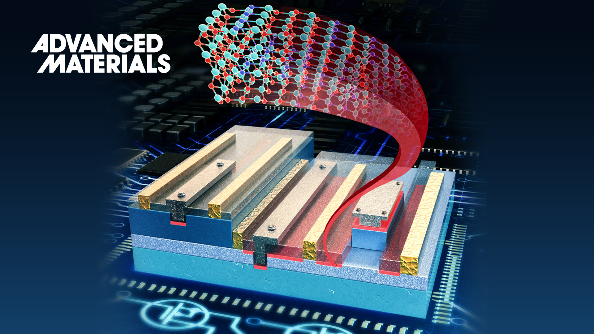
Assistant Professor Mengyuan Hua from the Department of Electrical and Electronic Engineering at the Southern University of Science and Technology (SUSTech) led a research work that reveals the formation and applications of lattice-aligned Gallium Oxynitride (GaON) nanolayer on GaN, which well passivate the GaN surface, and can further enhance the performance of GaN-based devices in various applications.
The results were recently published in Advanced Materials, entitled “Formation and Applications in Electronic Devices of Lattice-Aligned Gallium Oxynitride Nanolayer on Gallium Nitride”.
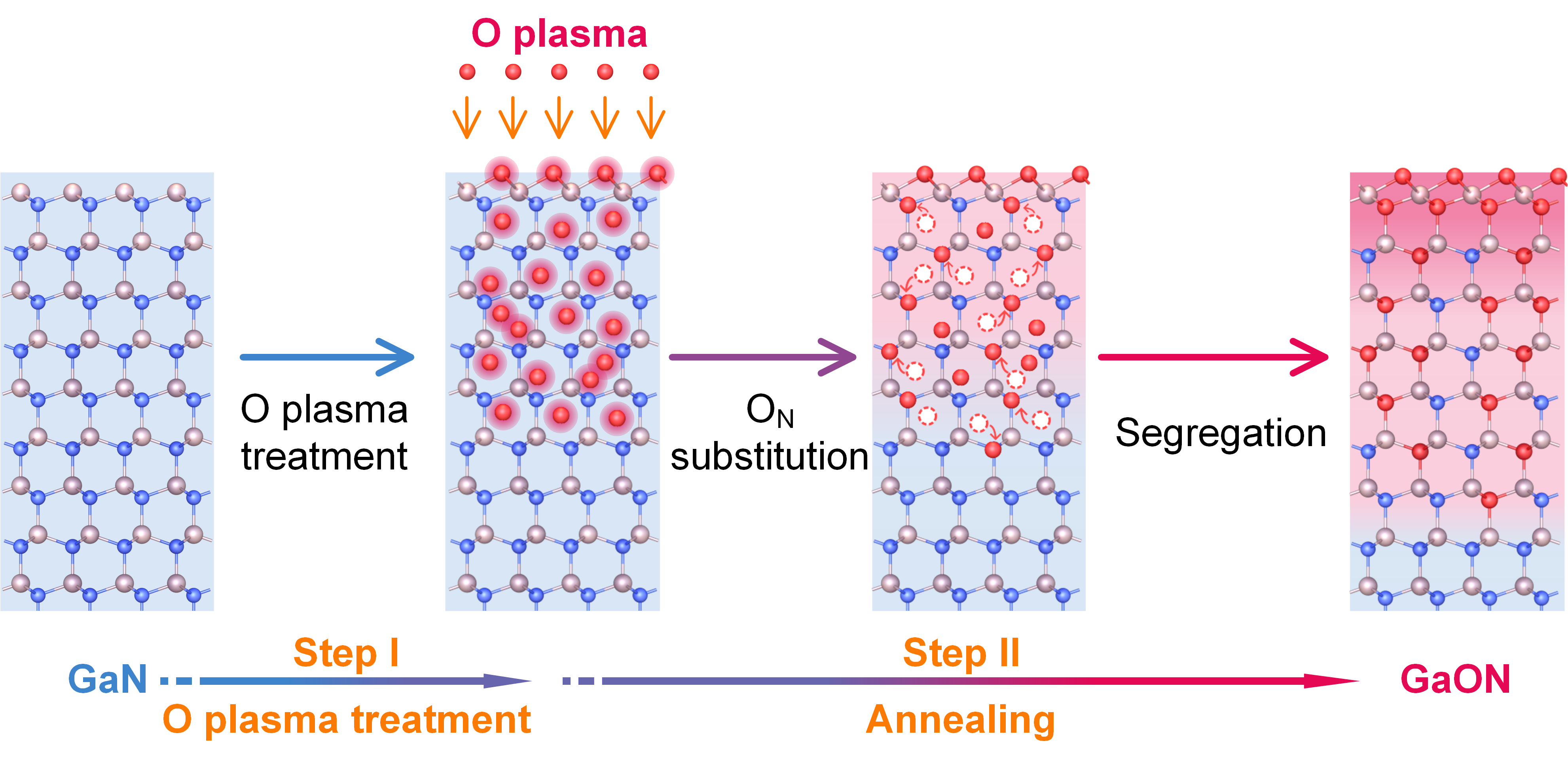
The researchers converted the GaN surface into a GaON epitaxial nanolayer through an in-situ two-step “oxidation–reconfiguration” process (Fig. 1). The O plasma treatment in the first step overcomes the chemical inertness of the GaN surface, and sequential thermal annealing manipulates the kinetic–thermodynamic reaction pathways to create a metastable GaON nanolayer with a wurtzite lattice. Further characterizations revealed the existence of two distinct high- and low-O-concentration layers. First-principles calculations have been applied to explain the experimentally observed bi-layer metastable GaON, which originated from the incomplete segregation of O in GaN.
Compared with GaO or other oxides, GaON has less lattice mismatch with GaN, so there is less interface state at GaON/GaN interface, making GaON more suitable for practical applications. The researchers demonstrated the use of GaON in two basic electrical devices (i.e., Schottky diodes and p-type transistors). GaON can suppress the reverse leakage of Schottky diodes and improve the gate control ability of p-type transistors. Nevertheless, the GaON nanolayer obtained from the experiments demonstrated reasonable uniformities, and is promising for mass production.

Figure 1. Formation of GaON nanolayer o GaN
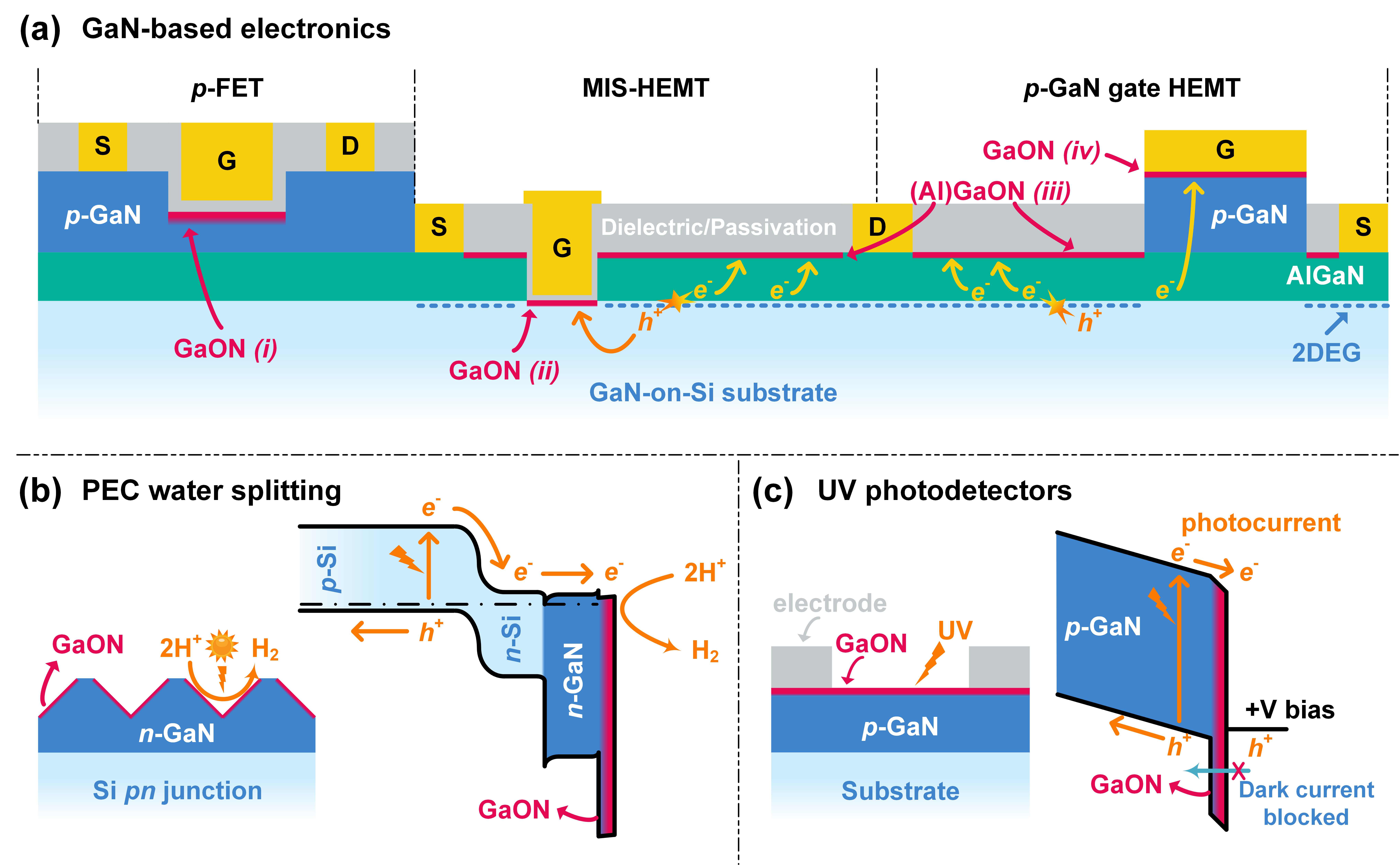
Based on the properties of GaON, and the capabilities of applying GaON on the GaN platform, the researchers further assessed the potential applications of GaON nanolayers in power devices, photoelectrochemical devices, and photodetectors (Fig. 2).

Figure 2. Applications of GaON nanolayers in (a) power devices, (b) photoelectrochemical devices, and (c) photodetectors
Junting Chen, a joint Ph.D. student of SUSTech and the Hong Kong University of Science and Technology (HKUST), and Research Asst. Prof. Junlei Zhao from the Department of Electrical and Electronic Engineering at SUSTech, are the co-first authors of this paper. Asst. Prof. Mengyuan Hua is the corresponding author.
This work was supported by the National Natural Science Foundation of China (NSFC), Guangdong Basic and Applied Basic Research Foundation, and Hong Kong-Macau Science and Technology Program (Category C) supported by the Shenzhen Science and Technology Innovation Committee.
Paper link: https://onlinelibrary.wiley.com/doi/10.1002/adma.202208960
To read all stories about SUSTech science, subscribe to the monthly SUSTech Newsletter.
Proofread ByAdrian Cremin, Yingying XIA
Photo By