The photovoltaic effect lies at the heart of eco-friendly energy harvesting. However, the conversion efficiency of traditional photovoltaic effect utilizing the built-in electric effect in p-n junctions is restricted by the Shockley-Queisser limit. Alternatively, intrinsic/bulk photovoltaic effect (IPVE/BPVE), a second-order nonlinear optoelectronic effect arising from the broken inversion symmetry of the crystalline structure, offers an effective approach to surpass this limit in traditional photovoltaic devices.
Van der Waals (vdW) layered materials meet all merits for IPVE investigations due to its low dimensionality, tunable bandgap, flexibility, easy manipulation, and rich species. Grain boundary (GB) widely exists in various vdW layered materials regardless of their crystalline symmetry, including graphene, MoS2, ReS2, and MoSe2. Meanwhile, GBs can introduce symmetry breaking in bulk materials without further symmetry requirements for the crystalline structure of bulk material. These properties make GB a promising platform for investigating IPVE.

Assistant Professor Xiaolong Chen’s research team from the Department of Electronic and Electrical Engineering at the Southern University of Science and Technology (SUSTech) recently discovered giant IPVE in one-dimensional van der Waals grain boundaries.
Their research work, entitled “Giant intrinsic photovoltaic effect in one-dimensional van der Waals grain boundaries”, has been published in Nature Communications.
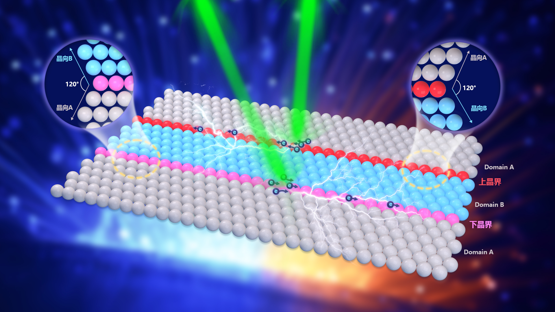
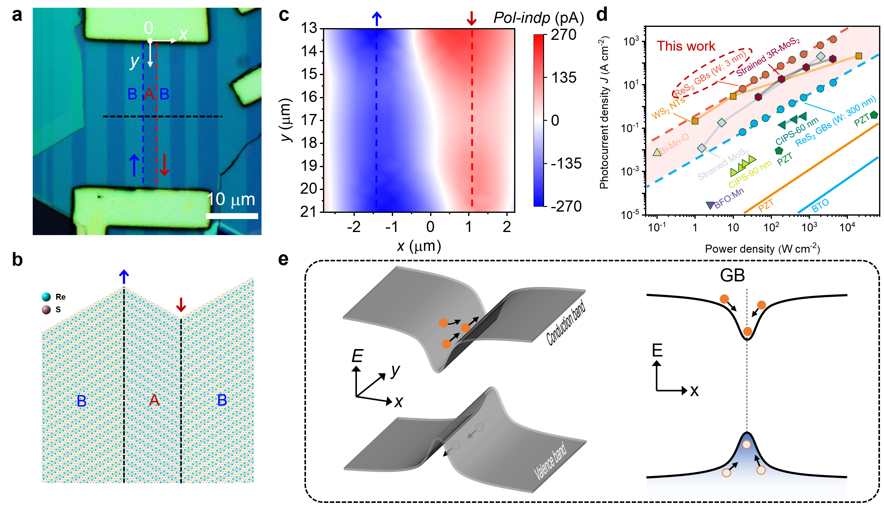
This study discovered strong IPVE in one-dimensional vdW GBs in a layered semiconductor, ReS2 (see Fig. 1). By characterization and symmetry analysis of crystalline orientations of the GBs, the authors found that the GB regions only show the two-fold rotation along the GBs (see Fig. 1b), which is distinct from the centrosymmetric crystalline structures in bulk ReS2. The lower geometric symmetry near GBs can support a strong DC photocurrent that propagates along GBs without any voltage bias (see Fig. 1b and c). The current density is among the highest values reported in various material systems.
The strategy is unique compared with previous research in the following aspects. Firstly, GBs widely exist in all kinds of materials and have a variety of configurations, which provides a capacious platform for IPVE and physics investigations. Secondly, GBs are embedded in bulk materials, and there is no symmetry requirement for the crystalline structure of bulk material to induce symmetry breaking in GBs. Thirdly, the formation of the quantum-well structure makes GBs a good one-dimensional system for IPVE investigation, which can effectively suppress carrier dissipation to other directions (see Fig. 1e). Fourthly, compared with edges, GBs with well-defined crystalline structures are free of dangling bonds. The reduced electron-defect scatterings in GBs with well-defined structures might suppress scatterings of photo-excited carriers and enhance IPVE photocurrent. Lastly, structures and densities of GBs can be generated and controlled through adjusting material growth conditions, which is important for making efficient optoelectronic devices.

Figure 1. (a) Optical image of a photodetector with multiple domains under polarized white light. Two adjacent subdomains are marked by A (red) and B (blue), respectively. Two adjacent GBs with reversed orientations are denoted by “↑” and “↓” and marked by blue and red dash lines, respectively. (b) Top view schematic of lattice structures near GBs. (c) Spatial distribution of the polarization-independent term of Short-circuit photocurrents (Iph). ↑ and ↓ GBs are marked by blue and red dash lines, respectively. (d) IPVE-induced photocurrent density in various materials. (e) Schematic of band diagram of ReS2 near GBs. Quantum well structures are formed along the x-direction.
Yongheng Zhou, a doctoral candidate at SUSTech, and Xin Zhou, a doctoral candidate at the National University of Singapore, are the co-first authors of this paper. Assistant Professor Xiaolong Chen, Research Assistant Professor Xianglong Yu of SUSTech, and Professor Jinshui Miao of the Chinese Academy of Sciences are the co-corresponding authors. SUSTech is the first communication unit of the paper.
The work was supported by the National Natural Science Foundation of China, Shenzhen Excellent Youth Program, Open research fund of State Key Laboratory of Infrared Physics, Shanghai Institute of Technical Physics, Chinese Academy of Sciences, Shenzhen Basic Research Program, Natural Science Foundation of Guangdong Province, Guangdong Major Talent Project, Fundamental Research Funds for the Central Universities, and Beijing Natural Science Foundation.
Paper link: https://www.nature.com/articles/s41467-024-44792-4
To read all stories about SUSTech science, subscribe to the monthly SUSTech Newsletter.
Proofread ByAdrian Cremin, Yingying XIA
Photo ByDepartment of Electronic and Electrical Engineering