Traditional perovskite materials hold promise for applications in solar cells, optoelectronic devices, catalysts, ferroelectrics, and quantum materials. In recent years, the emergence of 2D all-organic perovskites’ predecessors enriched the perovskite family and expanded its potential. However, synthesizing true 2D all-organic perovskites has remained unreported, stemming from the lack of design principles and synthesis methods.

A research team led by Associate Professor Junhao Lin from the Department of Physics at the Southern University of Science and Technology (SUSTech) and the Quantum Science Center of Guangdong-Hong Kong-Macao Greater Bay Area, in collaboration with a group led by Chair Professor Kian Ping Loh from the Department of Applied Physics at the Hong Kong Polytechnic University (PolyU), achieved a major breakthrough in the design, synthesis, and structure analysis of two-dimensional (2D) all-organic perovskites.
Their findings, published in the prestigious journal Science under the title “Molecularly thin, 2D all-organic perovskites”, address the challenge of unstable structure in 2D all-organic perovskites. By employing an innovative coordination strategy, the researchers successfully synthesized various 2D all-organic perovskite crystals, filling a gap in this field and holding significant value for enriching the perovskite material family.
The design of 2D all-organic perovskites faces two major challenges: charge balance and structural stability. These challenges involve the selection and site matching of large cation A, small cation B, and anion X. Professor Kian Ping Loh’s team proposed a new strategy, utilizing CMD+ as the A-site cation, NH4+ occupying the B site, and PF6– occupying the X site. They further introduced an additional NH4+ at the E site in the unit cell center’s interstitial space (Fig. 1).
CMD+ forms hydrogen bonds with the E-site NH4+ both horizontally and vertically, effectively balancing the charge and enhancing structural stability. Specifically, the lone pair at the nitrogen of CMD+ formed an N-H···N hydrogen bond with NH4+-edge laterally, whereas the chloromethane from the adjacent layer formed an N-H···Cl hydrogen bond with NH4+-edge vertically, thus stabilizing it by forming an NH4+-edge[PF6]3[N]2[Cl] octahedron. They also successfully synthesized a series of 2D all-organic perovskites with the A2B2X4 structure, such as CMD-N-P2 and BMD-N-P2, by replacing the CMD+ cation with the BMD+ cation.
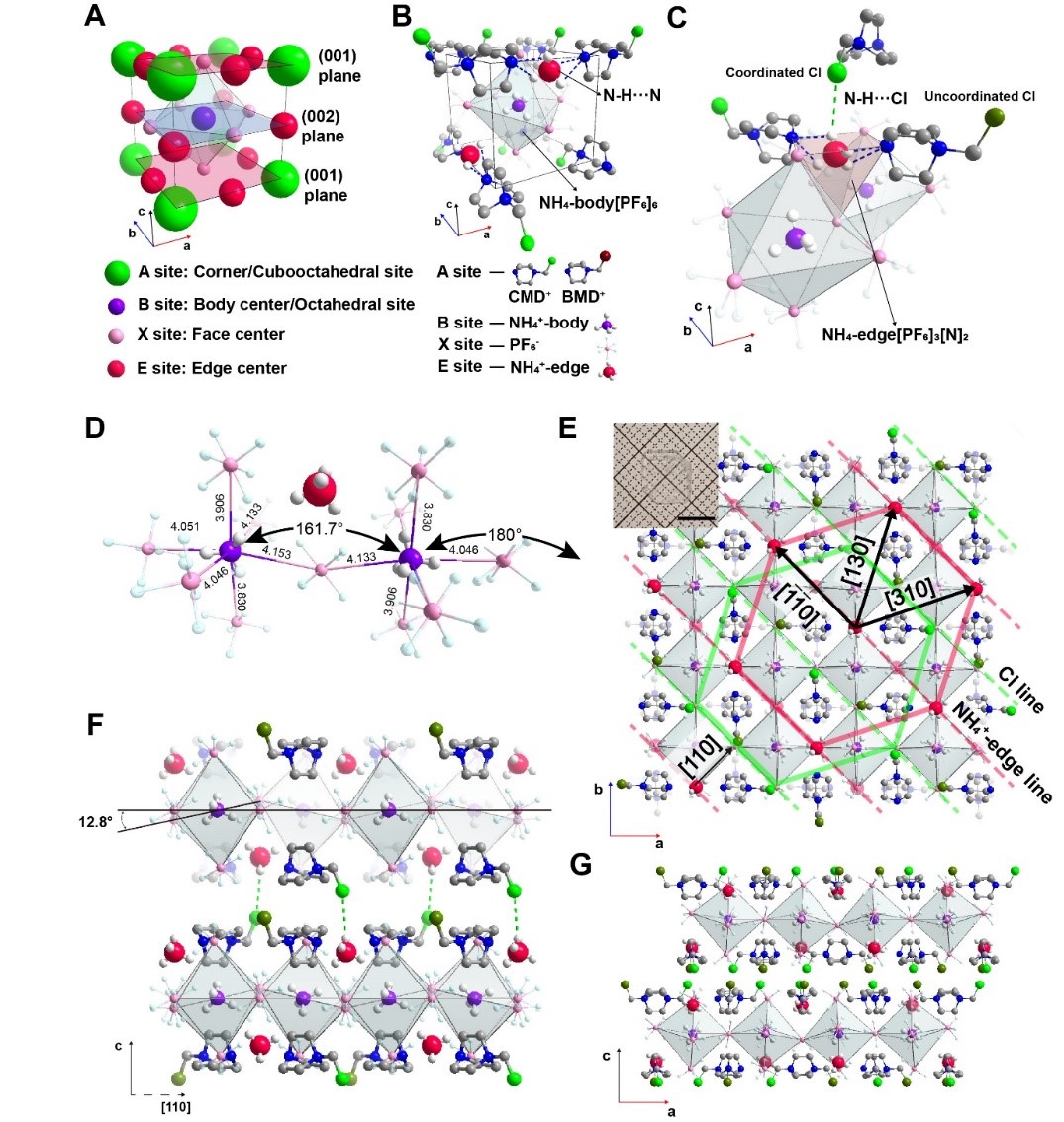
Figure 1. Structural description of CL-v phase 2D all-organic perovskite crystals
To directly confirm the perovskite-like assembly and arrangement of various molecules in this new material, high-resolution structural and elemental analysis is needed. High-resolution transmission electron microscopy (HRTEM) is an essential tool for this purpose. However, conventional TEM relies on accumulating a large number of high-energy imaging electrons to penetrate the sample and obtain high-resolution images. This high electron dose, typically reaching 105 electrons per square angstrom, makes it unsuitable for organic materials. Organic molecular materials, formed by light element covalent bonds and linked by weak hydrogen bonds, are similar to biological materials in their extreme sensitivity to electron beam damage. This sensitivity leads to rapid and irreversible structural changes under electron irradiation.
To overcome the limitations of conventional TEM for structural characterization of organic molecular materials, Associate Professor Junhao Lin’s team developed a cryogenic sample preparation technology and a cryogenic imaging method with ultra-low electron dose. Recognizing the sensitivity of organic molecules to radiation damage that increases with temperature, they first utilized the liquid nitrogen low-temperature environment of cryogenic TEM to suppress molecular thermal vibration and improve the tolerance dose of electron beam-sensitive materials.
To further minimize electron exposure, the team employed a high-detection efficiency direct electron counting camera along with a precise sample search method. In cooperation with Associate Professor Fang Lin’s team from South China Agricultural University (SCAU), a low-dose transmission image filtering algorithm was developed to perform fine filtering on the data. With this comprehensive approach, they finally achieved near-atomic direct imaging of 2D all-organic crystals at an ultra-low dose of about 1.1 electrons per square angstrom. This is five orders of magnitude lower than the electron dose required for conventional TEM atomic imaging while maintaining resolution, approaching the single electron dose imaging limit.
Figure 2 shows the organic groups connected by covalent bonds and the perfect cubic perovskite crystal structure driven by hydrogen bond assembly in the 2D organic perovskite single crystal. The electron energy loss spectrum test proves the chemical composition of the 2D organic perovskite.

Figure 2. High-resolution cryogenic structure and elemental characterization of CL-v phase 2D all-organic perovskite crystals
To demonstrate the effectiveness of the CL-v phase as a dielectric layer, the team of Assistant Professor Kai Leng from PolyU utilized dry transfer technology to fabricate a field-effect transistor (FET). A thin layer of CMD-N-P2 or BMD-N-P2 was transferred as the top gate dielectric layer onto MoS2, with Cr/Au metal serving as the source and drain electrodes.
The test results show n-type FET behavior in the transmission curves measured at different drain-source voltages (Vds). When Vds is set to 0.5 V, the on/off ratio surpasses 107, which is well above the standard of 104 required for actual logic circuits. The negligible hysteresis observed in the transfer curve suggests good contact between the all-organic perovskite dielectric layer and the inorganic 2D material channel. Additionally, the low subthreshold swing extracted from the transfer curve is 158 mV dec-1, which is lower than that of Al2O3 grown by atomic layer deposition. The output curve of the drain current-voltage (Id-Vd) exhibits linear characteristics at low bias (Figure 3).
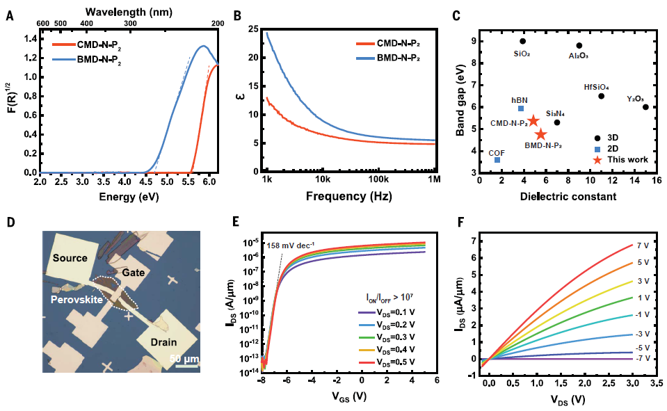
Figure 3. Dielectric properties of CL-v phase 2D all-organic perovskites and FET devices using CMD-N-P2 as the dielectric layer
This work introduces a new strategy for designing 2D all-organic layered perovskites. This strategy has enabled the successful synthesis of a variety of novel, ultra-thin, all-organic 2D crystals. These metal-free perovskite materials represent a new branch of perovskite research and provide a valuable foundation for the development of future all-organic 2D perovskite materials.
Crucially, cryogenic TEM proved instrumental in characterizing the crystal structure of these 2D all-organic perovskites. This technique provides researchers with a powerful tool to gain a deeper understanding of this new class of materials. Furthermore, it paves the way for the application of biological cryogenic TEM to characterize the organic groups within these chemical organic materials.
Hwa Seob Choi and Jun Lin, both postdoctoral fellows at PolyU, and Gang Wang, a postdoctoral fellow from the Department of Physics at SUSTech, are the co-first authors of the paper. Chair Professor Kian Ping Loh, Assistant Professor Kai Leng, and Assistant Professor Jun Yin from PolyU, along with Associate Professor Junhao Lin, are the co-corresponding authors.
This work was supported by the National Natural Science Foundation of China (NSFC), the “Pearl River Talent Plan” Innovation and Entrepreneurship Team, Shenzhen High-Level Talent Team, Shenzhen Municipal Government’s Stable Support for Universities, Shenzhen Key Laboratory, Quantum Science Center of Guangdong-Hong Kong-Macao Greater Bay Area, Guangdong Province Quantum Science Strategic Project, and the Cryo-Electron Microscopy Center of SUSTech.
Junhao Lin’s research group at SUSTech has consistently focused on developing innovative tools and core characterization technologies. Their productivity is evident: in just six months, they’ve published two papers in Nature and the above paper in Science. This success highlights the crucial role of mastering core characterization technologies in driving major scientific breakthroughs.
The group has several high-level papers under peer review, which are expected to further solidify the importance of advanced characterization technology. Additionally, the team is actively involved in the research and development of advanced characterization instruments for quantum technology at the Quantum Science Center of Guangdong-Hong Kong-Macao Greater Bay Area. Their goal is to develop new methods for tackling critical scientific challenges in contemporary quantum materials.
Paper link: https://www.science.org/doi/10.1126/science.adk8912
To read all stories about SUSTech science, subscribe to the monthly SUSTech Newsletter.
Proofread ByAdrian Cremin, Yingying XIA
Photo ByDepartment of Physics


