Advanced power semiconductor devices with high breakdown voltage and excellent reliability can enable power conversion systems with enhanced energy efficiency in addition to diminished size and cost. Power diodes based on GaN have great prospects thanks to their superior material properties. Yet, GaN-on-Si Schottky diodes (SBDs) are suffering from challenges in reverse blocking and device reliability. Additionally, the process of current GaN SBDs are less compatible with commercialized e-mode p-GaN HEMTs, therefore requiring significant additional efforts and costs in development and production.
A research group led by Assistant Professor Jun Ma from the Department of Electronic and Electrical Engineering at the Southern University of Science and Technology (SUSTech) has proposed a novel GaN Junction Barrier Schottky (JBS) diode. The devices are fully process-compatible with p-GaN HEMTs, showing great potential as a high-performance discrete power device and a building block for future ultra-compact and efficient all-GaN power solutions.
Their research, entitled “1200 V GaN-on-Si Junction Barrier Schottky (JBS) Diodes by An E-Mode-Compatible Process”, will be presented at the 2024 IEEE International Electron Devices Meeting (IEDM), a top conference in the field of electronic devices.

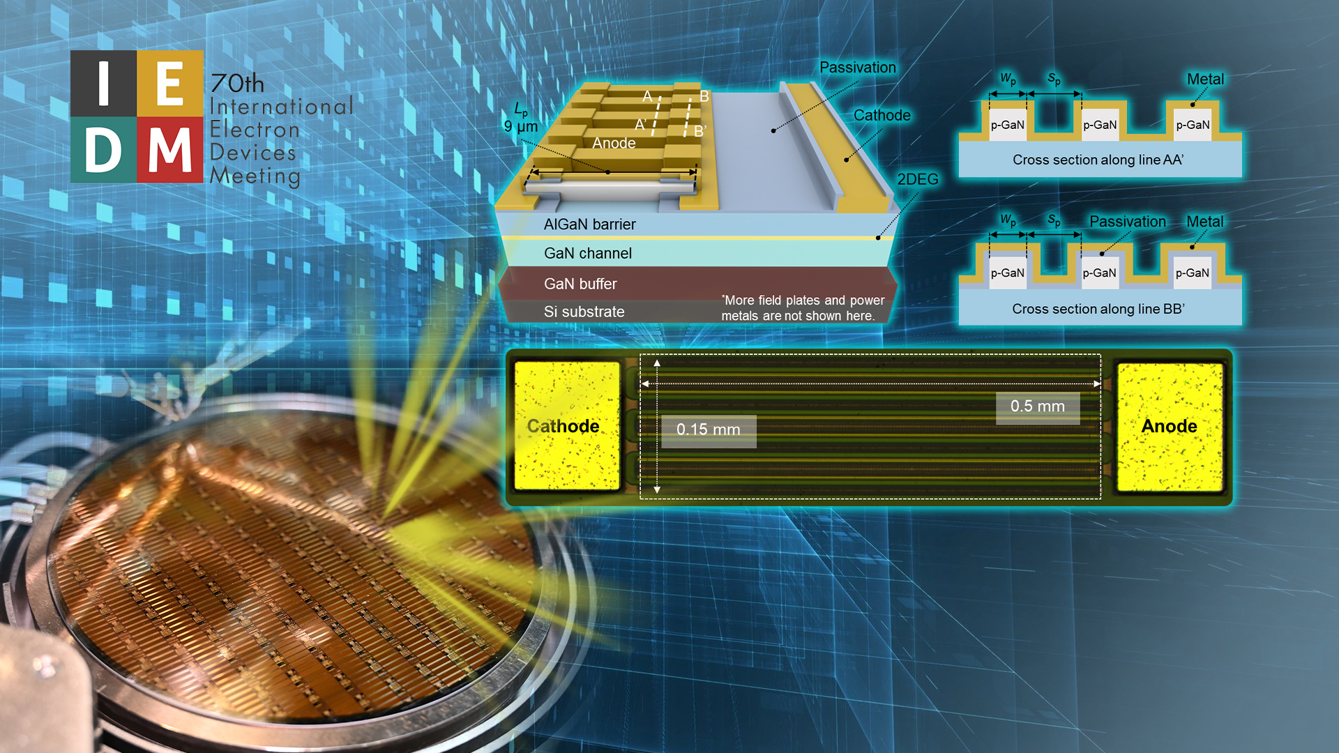
Figure 1. Schematics of the proposed JBS diode and an optical microscope image
The researchers developed a new GaN-on-Si JBS diode with high reverse blocking capability and high reliability based on the periodic p-GaN islands design. The fabrication process of the JBS diodes is fully compatible with the process flow of e-mode p-GaN HEMTs, therefore requiring little additional effort and costs. The p-GaN islands yield junction barriers at the Schottky junction and control the pinch-off voltage, reducing the device’s leakage current. The periodic p-GaN islands termination and field plate balance the peak electric field at the anode edge so that the device can withstand high voltages of more than 1200 V without breakdown.

Figure 2. The p-GaN islands regulate the pinch-off and improve the reverse blocking
Thanks to the advanced technical design, the JBS diodes present excellent characteristics in reverse blocking, forward conduction, switching, ESD/EOS, surge current, and high-temperature long-term reliability, and has broad application prospects for the realization of efficient and compact all-GaN power solutions in the future.

Figure 3. The excellent performance and reliability of the JBS diodes
Ph.D. student Wensong Zou at SUSTech is the first author of the paper. Assistant Professor Jun Ma is the corresponding author, with SUSTech serving as the first affiliated institution. Collaborating institutions include Shenzhen Pinghu Laboratory and Shenzhen Jingtong Microelectronics Co., Ltd.
Proofread ByAdrian Cremin, Yingying XIA
Photo ByDepartment of Electronic and Electrical Engineering