Optical patterning technology has garnered increasing attention in recent years for its significant applications in flexible electronics, optoelectronic devices, and micro/nano robotics. However, existing optical patterning techniques often rely on high-intensity light sources and complex optical systems, making them challenging for large-scale production due to high energy consumption and equipment costs. Thus, developing simple, efficient, and cost-effective patterning methods has become a critical focus in this field.
A research group led by Associate Professor Chengzhi Hu from the Department of Mechanical and Energy Engineering at the Southern University of Science and Technology (SUSTech) has made significant progress in the field of optical patterning of semiconductor nanoparticles.
Their research, titled “Light Patterning Semiconductor Nanoparticles by Modulating Surface Charges”, has been published in the journal Nature Communications.
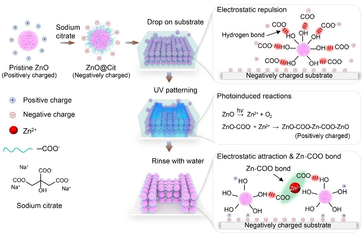
Figure 1. Scheme of positive patterning of ZnO@Cit nanoparticles
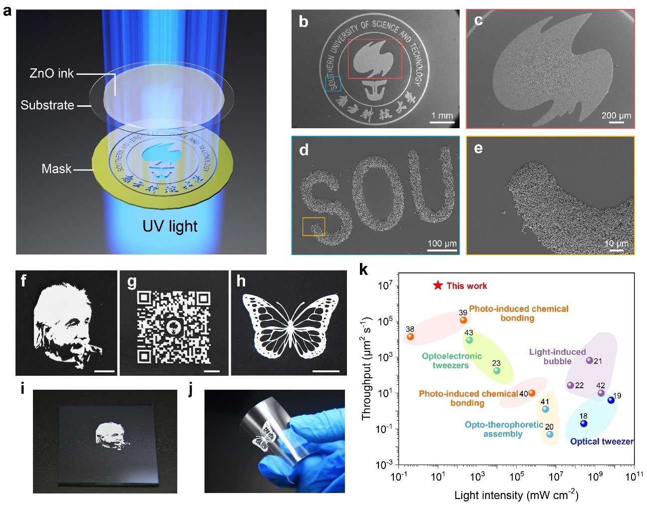
Figure 2. Results of positive patterning of ZnO@Cit nanoparticles
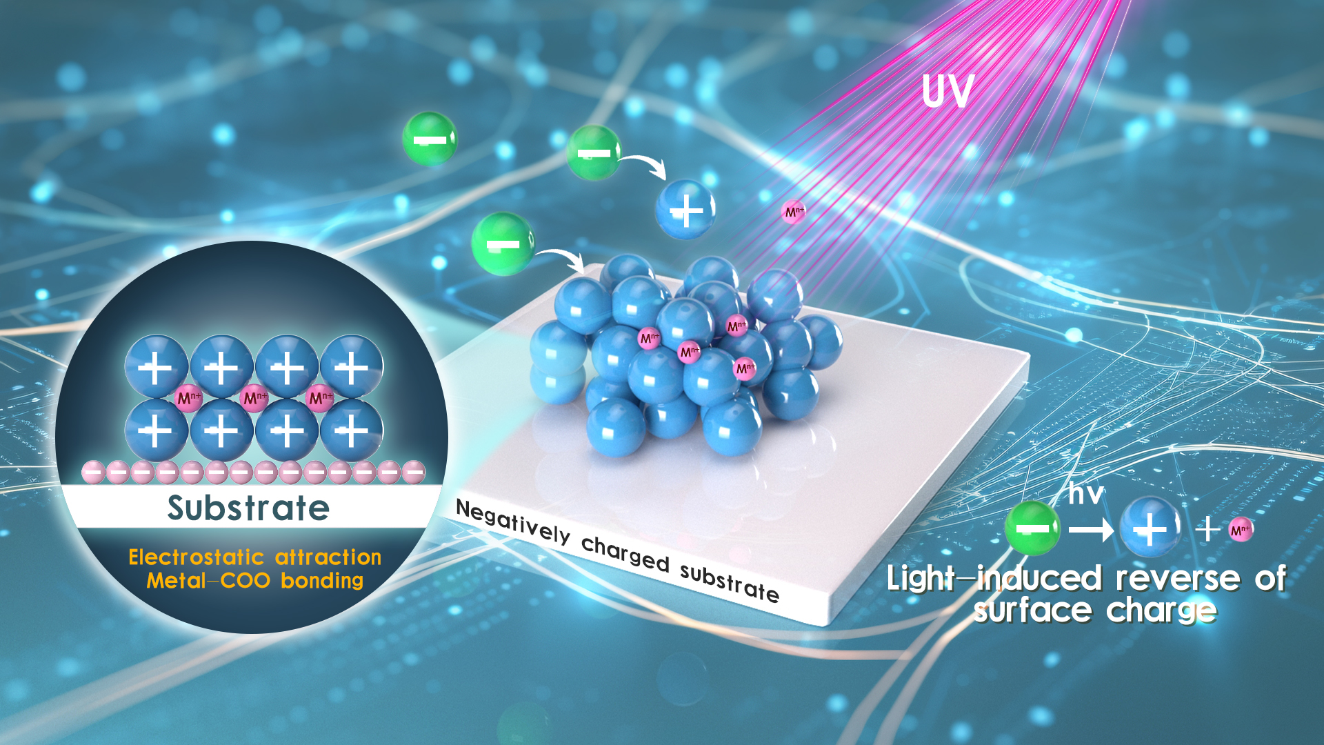
Professor Hu’s team proposed a novel method for semiconductor nanoparticle patterning based on light-induced surface charge modulation. By leveraging ultraviolet light (UV)-induced photodegradation of surface ligands on ZnO nanoparticles, they achieved significant changes in surface charges, enabling nanoparticle patterning on charged substrates through electrostatic interactions. This method enables the rapid, low-cost production of both positive and negative patterns.
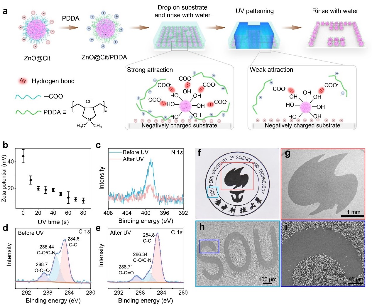
Figure 3. Negative patterning of ZnO@Cit/PDDA nanoparticles
The advantages of this method are as follows: First, compared to conventional laser-based techniques, it requires only 6 mW/cm² of light intensity and can generate centimeter-scale patterns within 10 seconds, significantly reducing energy consumption. Second, the approach eliminates the need for photoresists and is compatible with a wide range of substrates, including transparent glass and flexible PVC. Lastly, beyond ZnO, this method is also applicable to other semiconductor materials, such as ZnS, CdS, and TiO₂, showcasing its versatility across various material systems.
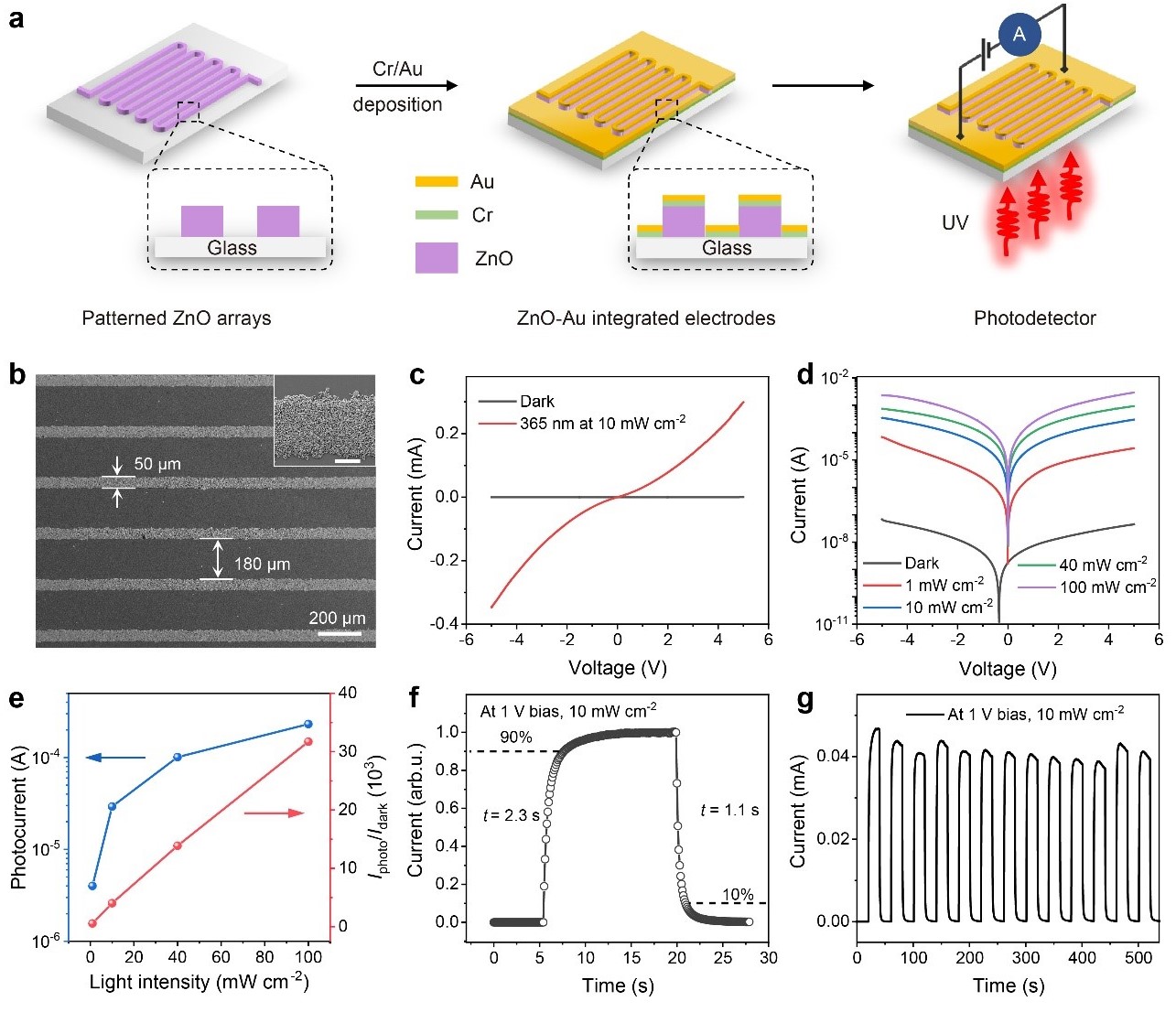
Figure 4. Photodetector made of patterned ZnO nanoparticles
The research team further demonstrated the application of this patterning technology by fabricating UV detectors based on ZnO nanoparticles. These devices exhibit outstanding optoelectronic performance, with a photo-to-dark current ratio exceeding 10⁴. This technology paves the way for scalable manufacturing of optoelectronic devices, highlighting its vast potential in smart devices, sensors, and beyond.
Ph.D. student Xiaoli He from the Department of Mechanical and Energy Engineering is the first author of this paper, with Dr. Hongri Gu from the University of Konstanz (now an Assistant Professor at The Hong Kong University of Science and Technology) as the second author. Associate Professor Chengzhi Hu and Professor Zhan Yang from Soochow University serve as the co-corresponding authors, and Associate Professor Liang Guo from SUSTech provided theoretical guidance for this work. SUSTech is the first affiliated institution for this paper.
Paper link: https://doi.org/10.1038/s41467-024-53926-7
To read all stories about SUSTech science, subscribe to the monthly SUSTech Newsletter.
Proofread ByAdrian Cremin, Yingying XIA
Photo ByDepartment of Mechanical and Energy Engineering