In recent years, the deployment of acoustic surface audio screens, which integrate sound and visuals, has gained much commercial popularity, particularly in large-screen organic light-emitting diode (OLED) televisions (TV), smartphones, microrobots, and wearable devices. By emitting sound directly from the screen surface, they offer more authentic and dynamic audio effects. Meanwhile, acoustic surface audio reduces the size of sound bars while maintaining an overall thin screen profile.
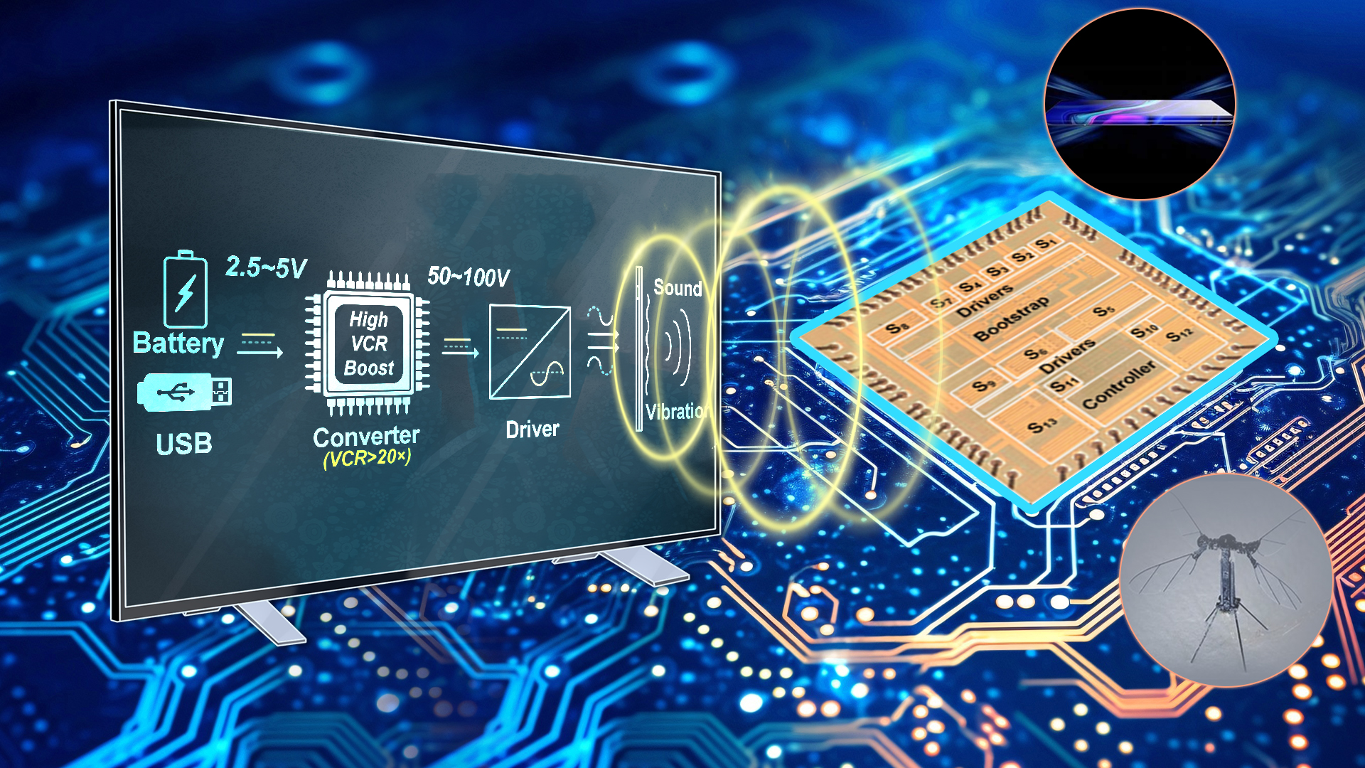
By eliminating traditional earpiece speakers, “zero-hole” screens enhance aesthetics while also improving the devices’ waterproof and dust resistance capabilities, greatly benefiting end users. Acoustic surface audio technology usually relies on piezoelectric thin-film actuators, which require high driving voltages (50–100 V) to ensure high-fidelity sound reproduction (Figure 1a). However, since these devices are typically powered by lithium-ion (Li-ion) batteries or standard universal serial bus (USB) power sources with a voltage range of 2.5-5V, the step-up DC-DC converters capable of delivering a voltage conversion ratio (VCR) larger than 20× are in high demand in these applications.
Associate Professor Junmin Jiang’s research group from the Department of Electronic and Electrical Engineering at the Southern University of Science and Technology (SUSTech) has made significant progress in the field of hybrid step-up power converters.
Their paper, titled “A 2.5–5-V Input 100-V Output 86.2% Peak Efficiency Fibonacci-Dickson Hybrid Converter for Acoustic Surface Audio Driver”, has been published in the IEEE Journal of Solid-State Circuits (JSSC), a leading journal in integrated circuit design.
Achieving a high VCR poses significant challenges for conventional boost topologies. These include the need to achieve extremely short ON-time pulse for switches, as well as overcoming issues such as low power efficiency, low power density, and increased reliability risks. On the other hand, traditional switched-capacitor converters (SC), such as Fibonacci and Dickson topologies (Figure 1b), can easily achieve high VCR. However, they still face challenges in achieving high density, as they require a large number of capacitors and high voltage switches. Additionally, maintaining high efficiency with discrete VCRs over wide voltage ranges is difficult.
To address these issues, recent hybrid boost converters have been proposed. These use an SC topology at the back end to lower the high output voltage stress across power switches, and an inductor-based topology at the front end for current delivery and continuous VCR. Among the various hybrid boost topologies, the reverse double-step down (RDSD) converter with two inductors was widely used (Figure 1b). This design features automatic inductor current balancing in two branches and soft charging of the flying capacitor. However, the VCR of the RDSD converter is limited, achieving a maximum VCR of only 4 with a duty ratio (D) of 0.5.
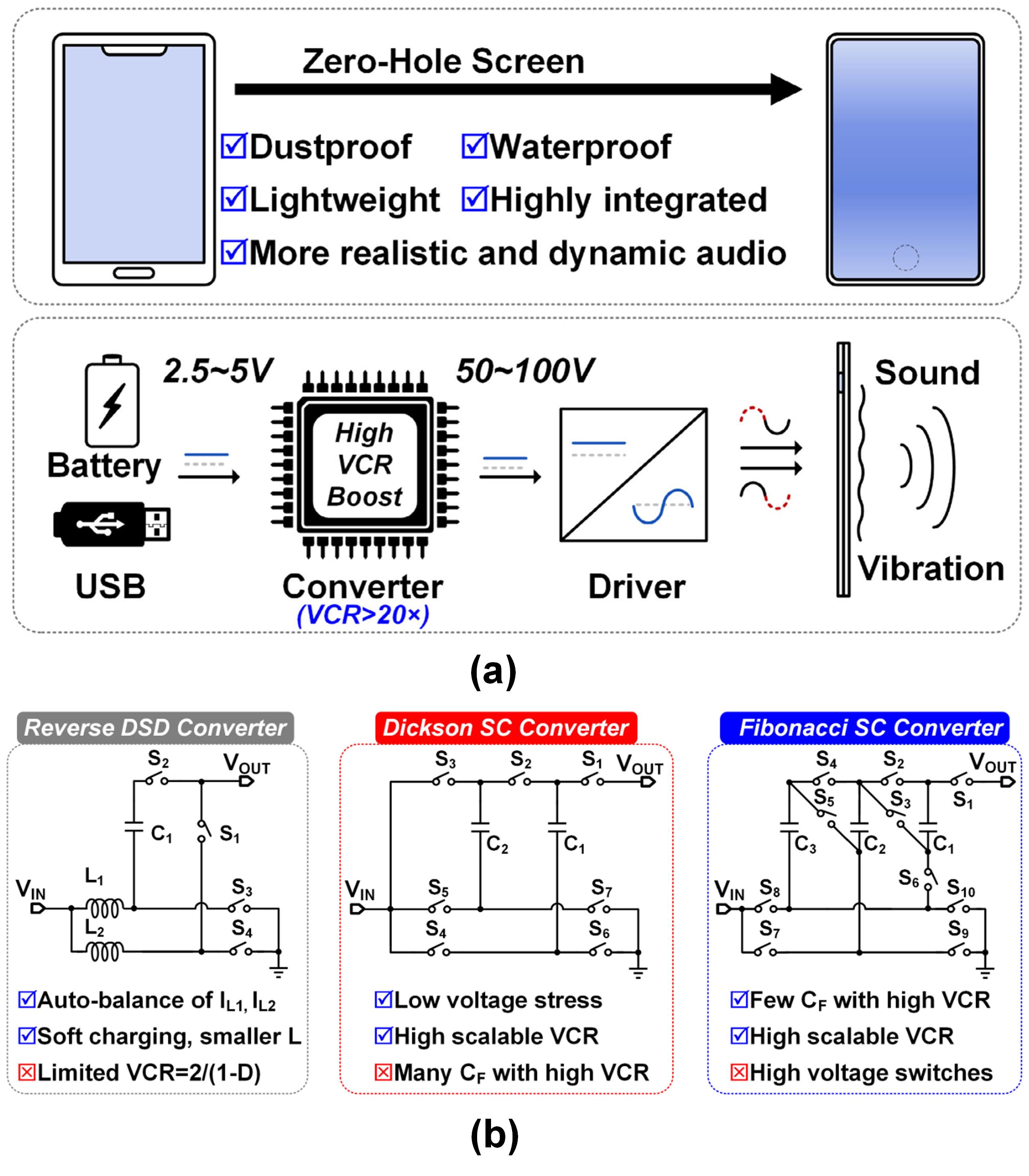
Figure 1. (a) Acoustic surface application of high VCR boost converters; (b) Classical hybrid and SC topologies
The researchers proposed a Fibonacci-Dickson hybrid boost (FDHB) converter, based on an RDSD converter that utilizes a cascaded approach with merged Fibonacci and Dickson SC topologies. This topology can achieve an extremely high VCR while retaining the inherent advantages of these two topologies, such as lower switch voltage and fewer flying capacitors. However, due to the limitations of the BCD process, the parasitic bipolar transistors generated leakage currents, which greatly degraded the overall power efficiency. To overcome this, the FDHB converter was implemented using a silicon on insulator (SOI) process, which improved reliability and efficiency.
The design of the number of stages in both the low-side Fibonacci and high-side Dickson SC topologies was carefully optimized to achieve a better tradeoff (Figure 2a). The low-side Fibonacci topology achieves a high VCR with fewer flying capacitors and switches. On the high-side near the output, a 2-stage Dickson is employed to further enhance the VCR while mitigating the voltage stress of capacitors and power switches at the output. This topology achieves the lowest voltage-current stress among the state-of-the-art step-up converters, resulting in a 70% reduction in stress compared to a conventional boost converter, and a high VCR of 20 with D of 0.5 (Figure 2b).
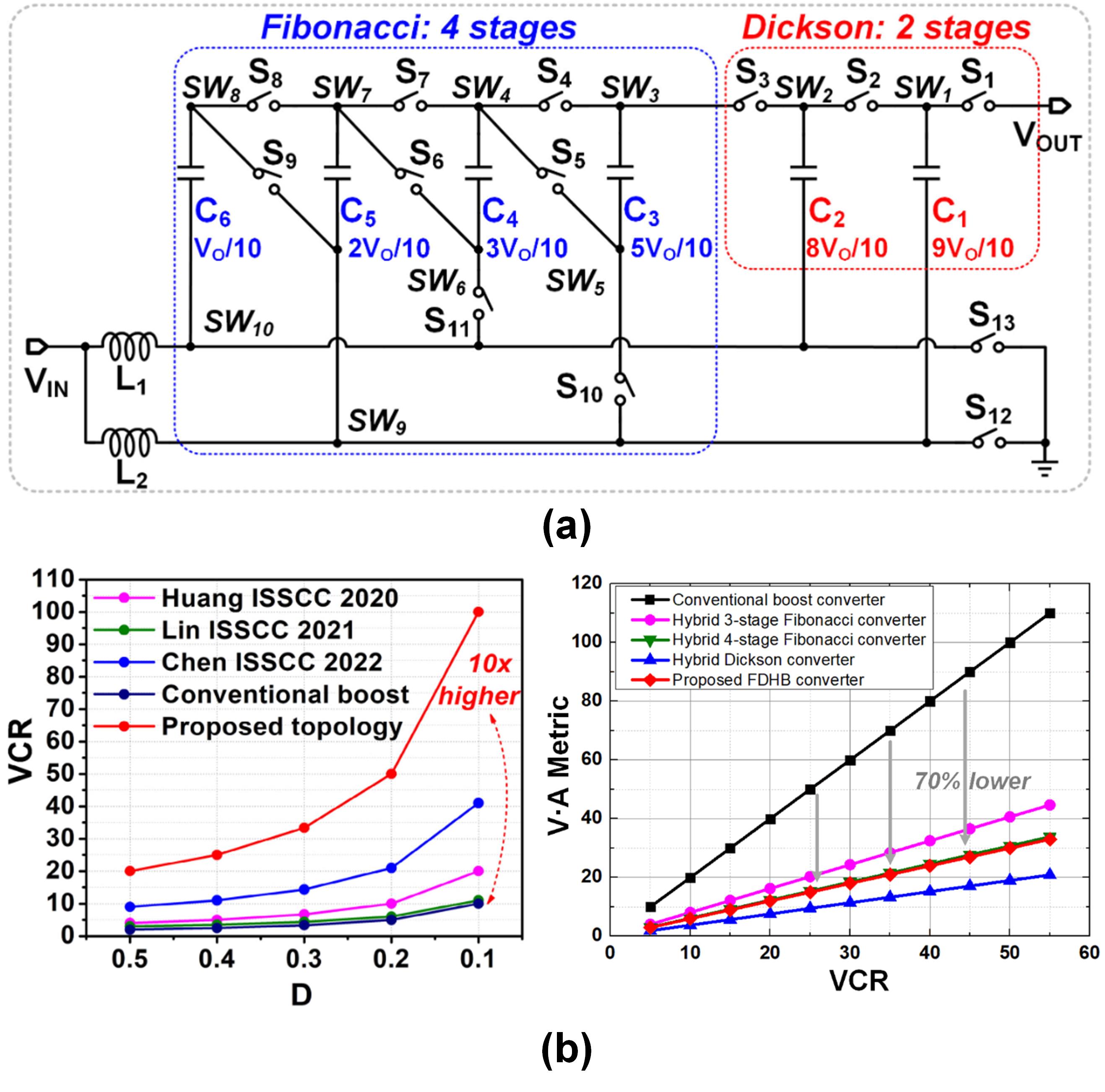
Figure 2. (a) The proposed high VCR step-up converter FDHB; (b) Comparison with previous works
The proposed FDHB converter uses a stacked active bootstrap to replace the conventional bootstrap diode with an actively controlled transistor with lower turn-on resistance. This overcomes the issue of diode forward voltage drop and effectively drives all power switches, thereby improving power efficiency. The converter was fabricated in a 180-nm SOI process. The chip micrograph and PCB photograph are shown in Figure 3a.
Measured results demonstrate that the converter achieves an input voltage range of 2.5-5V, a maximum output voltage of 100V, and a maximum output power of 2W. It also delivers a peak efficiency of 86.2% and a power density of 7.43 W/cm³ (Figure 3b). A 20ns load current step (from 1mA to 10mA) results in only a 2.5‰ output voltage fluctuation, with recovery times of 40μs (undershoot) and 62.5μs (overshoot), exhibiting excellent dynamic performance (Figure 3c). The proposed FDHB converter achieves both high efficiency and a maximum VCR of up to 40, representing the best performance among recent high VCR step-up converters.
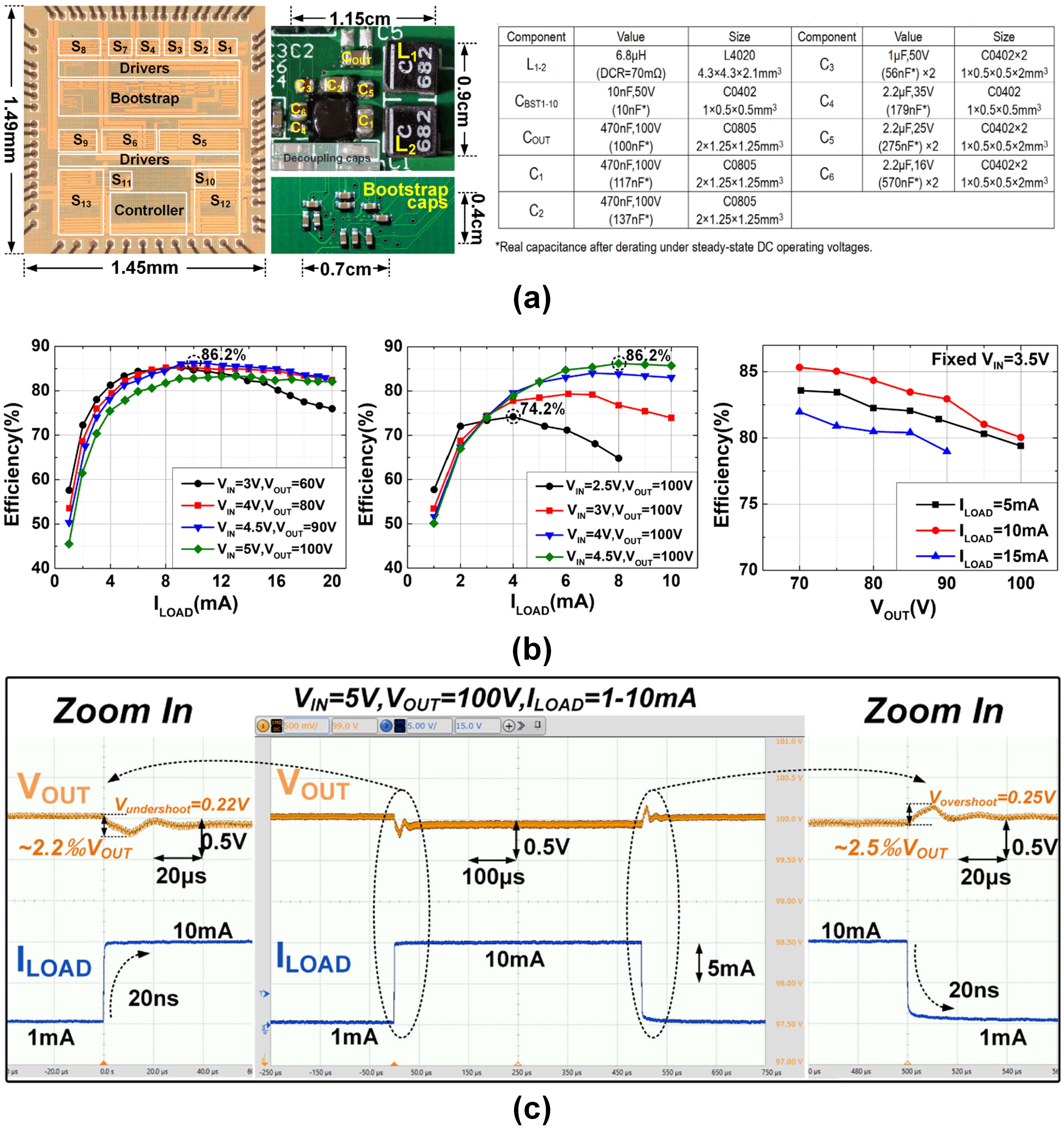
Figure 3. (a) Chip micrograph and PCB photograph; (b) Measured efficiency versus input and output conditions, VCR conditions, and load conditions; (c) Measured load transient response waveforms
Visiting Ph.D. student Yifan Jiang from Junmin Jiang’s research group is the first author of the paper. Associate Professor Junmin Jiang and Professor Yan Lu from Tsinghua University are the co-corresponding authors. SUSTech is the first affiliated institution.
Paper link: https://ieeexplore.ieee.org/document/10892274
To read all stories about SUSTech science, subscribe to the monthly SUSTech Newsletter.
Proofread ByAdrian Cremin, Yilin ZHOU
Photo ByDepartment of Electronic and Electrical Engineering


