Power integrated circuits (ICs) play a vital role in modern electronics, converting energy efficiently for everything from high-resolution displays to advanced sensors. As devices become faster, smaller, and more power-demanding, traditional converter designs are reaching their limits in efficiency and response speed. New approaches to converter design are helping to overcome these challenges, delivering compact and flexible solutions that can meet the needs of next-generation technologies such as MicroLED displays, LiDAR, and high-speed sensing. These developments mark an important step toward more adaptable and energy-efficient electronic systems.
A research team led by Associate Professor Junmin Jiang from the Department of Electronic and Electrical Engineering at the Southern University of Science and Technology (SUSTech) has achieved significant progress in high-density DC-DC converter integrated circuits. Their latest findings have been published across three leading journals and international conferences, including IEEE Transactions on Power Electronics (TPEL), IEEE Transactions on Circuits and Systems I: Regular Papers (TCAS-I) , and the 2025 IEEE Custom Integrated Circuits Conference (CICC).
Advanced DC-DC converter design for next-generation MicroLED displays
With the advancement of display screen pixel resolution, single-pixel dimensions have shrunk from over 1 mm to just several tens of micrometers, while the turn-on voltage of light-emitting diodes (LEDs) has decreased from over 10 V to below 4 V (Figure 1). To employ low-voltage driving devices ensuring display refresh rates, the power supply voltage must also be minimized, requiring negative-voltage power sources.
Traditional negative-voltage converters predominantly target higher-voltage-drop OLEDs, typically employing inverting buck-boost (IBB) or inverting boost converters. Due to topological limitations, these struggle to achieve rapid dynamic responses and face constraints with high voltage conversion ratios, thereby limiting their application in advanced MicroLED displays.
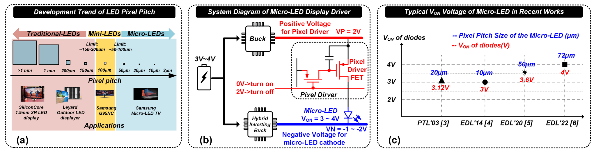
Figure 1. Application schematic diagram of the negative-voltage buck converter
The research team proposed a hybrid inverting buck (HIB) converter that innovatively integrates a -1× switched-capacitor (SC) network with a buck converter. This topology requires only three power switches, one flying capacitor, and one inductor, achieving an adjustable negative output voltage from -1 to -2 V with a 3-to-4 V input (Figure 2). Compared to traditional inverting buck-boost (IBB) and Cuk converters, the design offers three key advantages: a smaller footprint where its power stage requires only two off-chip components; a continuous output current that enables faster load transient response; and the absence ofright-half-plane zeros (RHPZs) that simplifies loop compensation design.
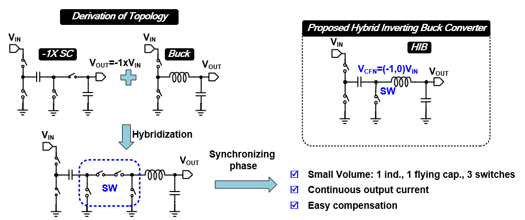
Figure 2. Proposed topology of the hybrid inverting buck (HIB) converter
The HIB converter achieves an adjustable -1 to -2V output from a 3–4 V input, a maximum output current of 2.2 A, peak efficiency of 92.9%, volumetric power density of 295 mW/mm³, and a dynamic response time of just 5μs (Figure 3).
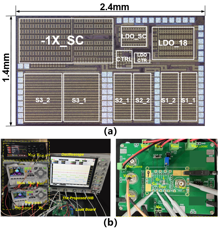
Figure 3. (a) Packaged die micrograph and (b) test setup/PCB photograph
This work, titled “Design and Analysis of a Hybrid Inverting Buck Converter with 5μs Response Time and 92.9% Efficiency for Micro-LED Displays,” has been published in the top-tier power electronics journal IEEE TPEL.
Graduates Xingfa Yan and Gang Liu from SUSTech are the co-first authors of this paper. Associate Professor Junmin Jiang, Research Assistant Professor Chen Hu from the Department of Electronic and Electrical Engineering at SUSTech, and Assistant Professor Xun Liu from The Chinese University of Hong Kong serve as the co-corresponding authors SUSTech is the first affiliated institution.
High VCR step-up converter for LiDAR driver applications
With the widespread adoption of Internet of Things (IoT) devices, high-efficiency power management systems have become crucial for extending device lifespan and reducing maintenance costs. Taking laser sensors powered by photovoltaic panels as an example, conventional solutions employing two-stage boost converter architectures typically exhibit system efficiencies below 70%, while suffering from large form factors and high costs.
To achieve single-stage voltage boosting and enhance system efficiency, recent research has focused on single-stage boost converter topologies with high step-up ratios. However, most existing studies rely on two-phase operation modes, constraining the achievable voltage conversion ratios. Such approaches generally require over five flying capacitors to attain merely 10-20× step-up ratios.
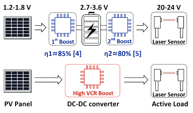
Figure 4. Application diagram of a laser sensor module directly powered by photovoltaic panels
To enhance the power density of boost converter topologies, the researchers innovatively proposed a single-stage four-phase hybrid boost converter architecture. This design achieves an 11-to-20× voltage conversion ratio (VCR) using only three flying capacitors and one inductor, directly elevating photovoltaic voltages from 1.2-1.8 V to the 20-24 V operating range required by LiDAR systems.
They illustrated the operating modes of the proposed converter topology, where three capacitors are switched to attain a 10× step-up gain—the maximum achievable ratio with three capacitors—while incorporating a switched-inductor technique to enable adjustable output voltage and reduce charge/discharge losses in switching capacitors (Figure 5). Compared to conventional boost converters, this topology reduces average inductor current by ~55% and inductor current ripple by 52%, significantly diminishing inductor size requirements.
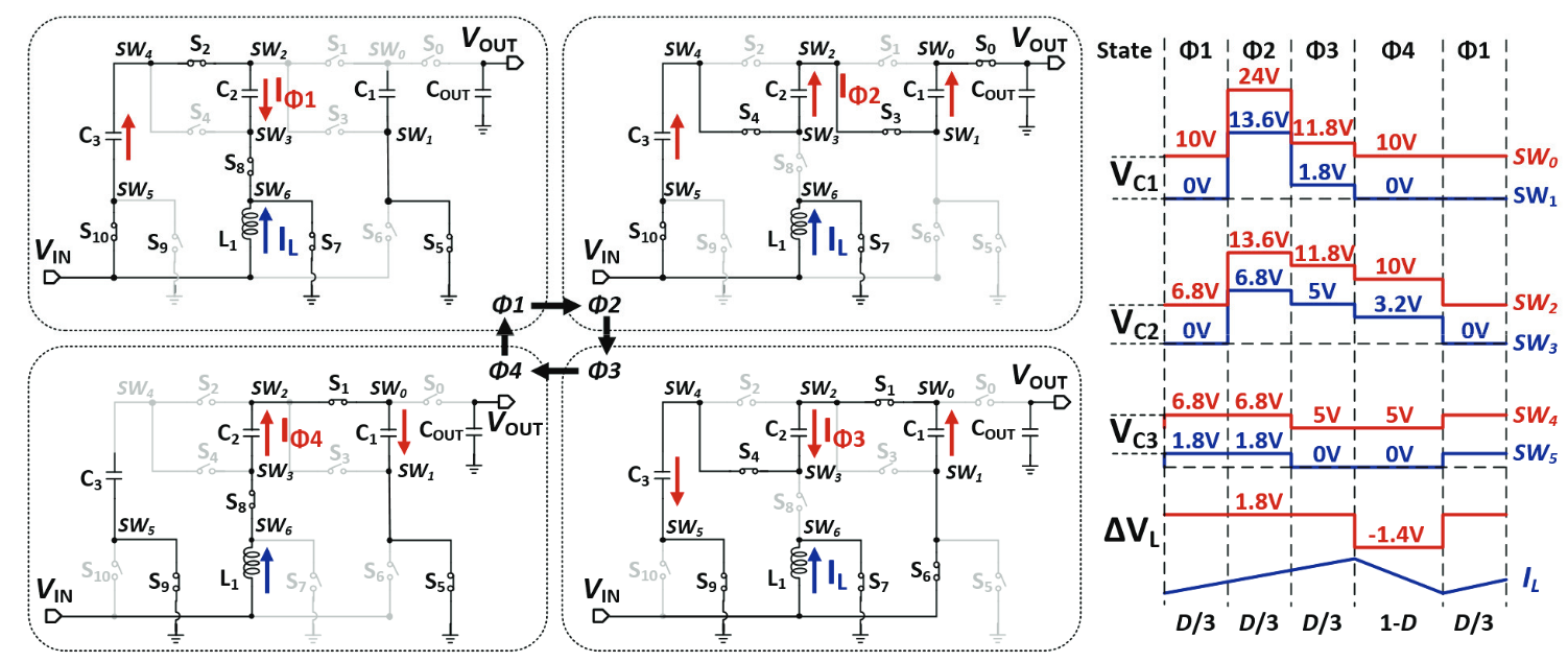
Figure 5. Schematic diagram illustrating the operation modes and corresponding voltage/current waveforms of the converter
Fabricated in a 0.18-μm process, the IC occupies just 2.23-mm². Operating with a 1.2-to-1.8V input, it achieves a 20-to-24V output with an 11-to-20× voltage conversion ratio, attaining 76.7% peak efficiency and 12-mW/mm³ power density.
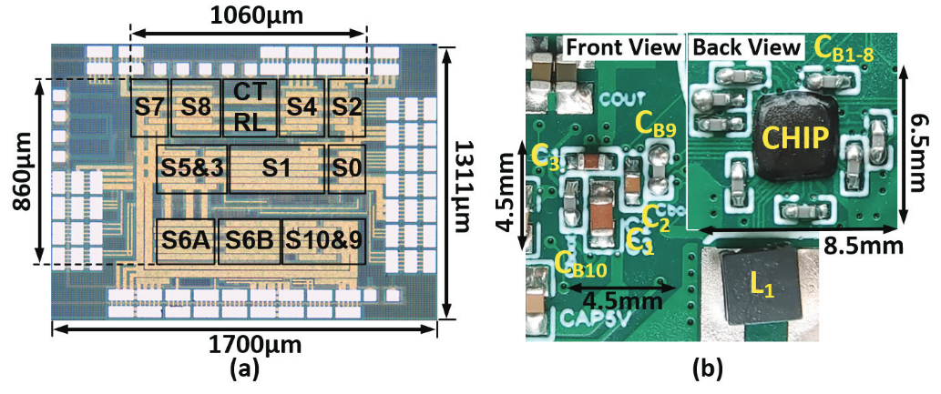
Figure 6. (a) Packaged die and (b) PCB photograph
This work, titled “A Single-Stage Four-Phase Hybrid Boost Converter With 11-to-20 VCRs for LiDAR Driver Applications,” has been published in IEEE TCAS-I.
Research Assistant Professor Chen Hu is the first author of this paper, with Associate Professor Junmin Jiang as the corresponding author. SUSTech is the first affiliated institution.
Wide-output-range switched capacitor converter for high-speed displays and sensors
High-speed, high-density DCDC boost converters are widely used in display and sensing technologies. However, power inductors in traditional boost topologies impose fundamental limitations on system power density and transient response speed. At the 2025 CICC, the research team unveiled a sigma switched-capacitor (SC) boost converter that achieved breakthroughs in power density and transient performance. Nevertheless, its fixed output voltage constrains application flexibility.
To address the critical limitation of fixed conversion ratios in switched-capacitor (SC) topologies—which narrows application scope—this work proposes a wide-output-range SC sigma converter architecture and chip design. The IC architecture combines a reconfigurable switched-capacitor network at the high-voltage output stage with a high-bandwidth LDO at the low-voltage input stage (Figure 7). The SC network switches its conversion ratio between 3× and 4× Vin, while the LDO’s input stage toggles between 1× and 0.5× Vin. This cascaded configuration achieves over 10× wider output voltage range compared to fixed-ratio SC converters reported at ISSCC 2024, while the LDO simultaneously delivers rapid, high-precision dynamic voltage regulation.
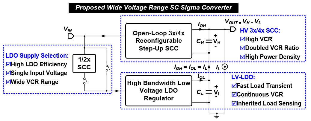
Figure 7. Wide-output-range SC sigma converter
When the SC network operates in 3-phase mode, it achieves a 4× step-up gain; in 2-phase operation, it delivers a 3× voltage boost (Figure 8). Combined with the LDO’s continuously variable voltage regulation capability, the converter achieves a 12.6-24 V output range—10.4× wider than the sigma switched-capacitor (SC) boost converter presented at ISSCC 2024.
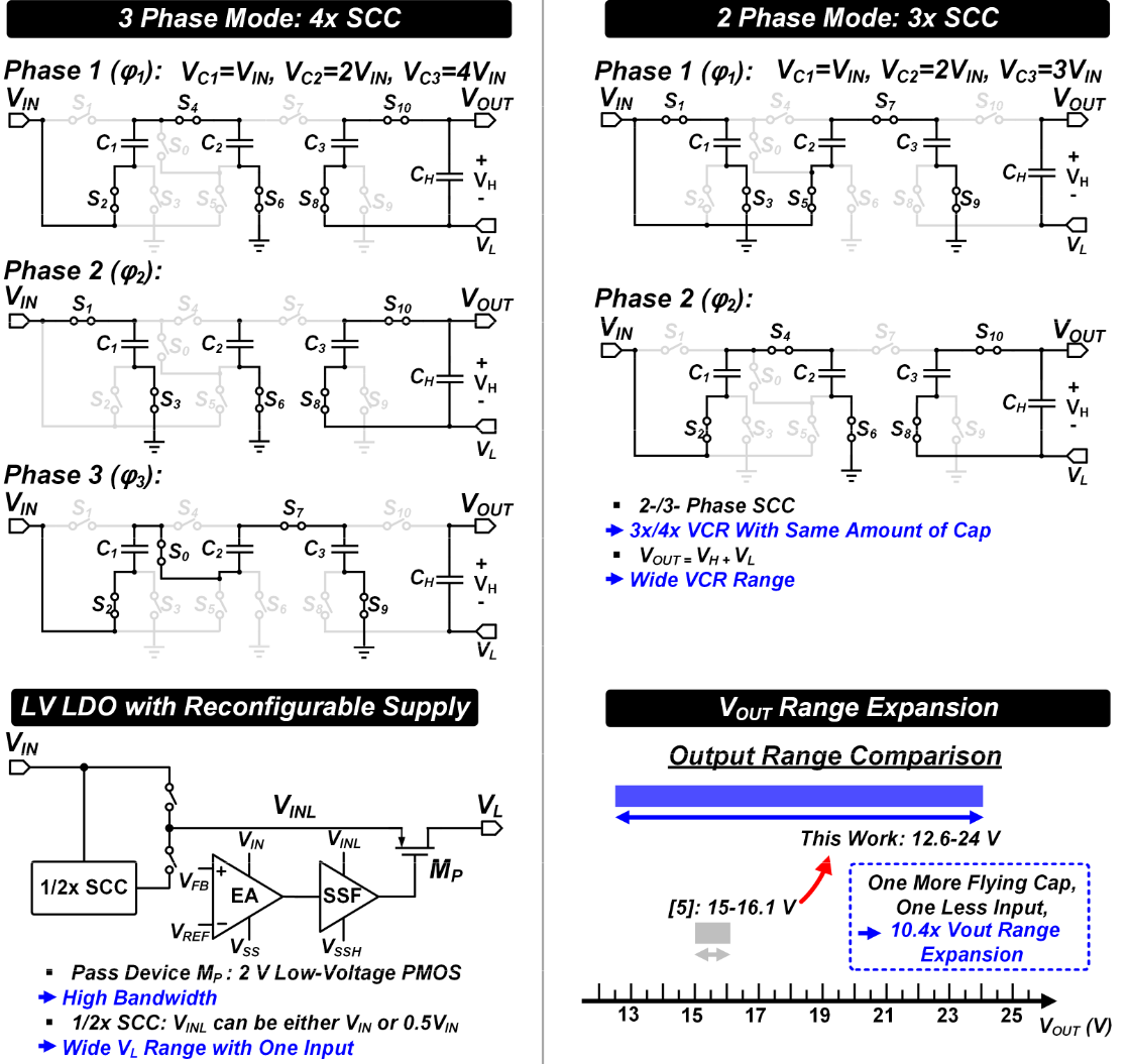
Figure 8. Schematic diagram illustrating the power-stage operating principle and output voltage-range-extension efficacy
Fabricated and validated in a 0.18-μm process, the IC achieves a maximum output power of 6.87 W under a 3.7-5V input and 0-300 mA output current. It demonstrates 95% peak efficiency at 4.18 W output, an ultrafast 350 ns load transient response time from 0-200 mA, and a power density of 179 mW/mm³.
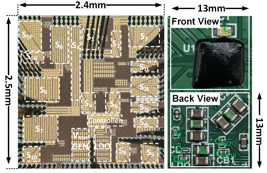
Figure 9. Packaged die and PCB prototype photographs
This work, titled“A 6.87W 3.7-5V Input 12.6-24V Output Switched-Capacitor Sigma Converter with Multiple Voltage Domains,” was presented at the 2025 IEEE CICC.
Visiting student Lingfeng Zhu from the Department of Electronic and Electrical Engineering at SUSTech is the first author of the paper, with Associate Professor Junmin Jiang as the corresponding author. SUSTech is the first affiliated institution.
Paper links (In order of appearance above):
IEEE TPEL: https://ieeexplore.ieee.org/document/11059803
IEEE TCAS-I: https://ieeexplore.ieee.org/document/11048654
2025 IEEE CICC: https://ieeexplore.ieee.org/document/10983553
To read all stories about SUSTech science, subscribe to the monthly SUSTech Newsletter.
Proofread ByAdrian Cremin, Yifei REN
Photo ByDepartment of Electronic and Electrical Engineering


