The interconnects between quantum processors and control electronics can be made more compact and reliable by placing classical circuits at cryogenic temperature (CT) closer to that of qubits. Low ambient temperature is also favorable for lowering the noise of electronics, which is critical for quantum computing applications.
Signal sources are critical blocks in both the control and readout circuits for quantum computing systems. Qubit control requires microwave signals modulated by baseband arbitrary waveform envelopes to generate 10ns-to-100ns periodic pulsed signals to manipulate the qubit state.
In order to prevent qubit state dephasing, the carrier should have a precision better than 1.9kHz (rms). To ensure scalability, signal sources should be tunable in a wide range, assuming enough margin to adapt to PVT variations. Although harmonic-rich tanks have been employed in designs to suppress flicker noise, the 1/f corners were still easily increased from hundreds of kHz at room temperature (RT) to several MHz at CT. The deterioration of 1/f noise for VCOs can cause difficulties in cryo-CMOS PLL designs for quantum interface applications.
Associate Professor Yatao Peng from the Shenzhen Institute for Quantum Science and Engineering (SIQSE) at the Southern University of Science and Technology (SUSTech), in collaboration with Professor Edoardo Charbon from the Advanced Quantum Architecture Laboratory (AQUA Lab), are working on a cryogenic (Bi)CMOS integrated circuit for quantum applications to solve the scalable control/readout problem for large-scale qubits.
Recently, they proposed a cryogenic hybrid class B/C mode-switching VCO structure, which solves the flicker noise degradation problem of cryo-CMOS VCOs, thus paving the way to achieve a fully integrated quantum readout/control chip.
Their research, entitled “A Cryogenic SiGe BiCMOS Hybrid Class B/C Mode-Switching VCO Achieving 201dBc/Hz Figure-of-Merit and 4.2 GHz Frequency Tuning Range,” has been presented at the premier conference IEEE International Solid-State Circuits Conference 2022 (ISSCC).

Figure 1. Hierarchical structure of quantum computing system with room/cryogenic temperature readout and control electronics.
The proposed VCO designed in 130 nm SiGe BiCMOS technology is reported in this work. A dual-mode LC tank implemented by coupled inductors is proposed for the VCO design. The two-coupled oscillating cores are biased in class-B and class-C mode, respectively. The Class C VCO achieves better current efficiency and figure of merit (FoM). At the same time, the class B VCO ensures a robust startup without extra startup circuits, saving power consumption further.
The common-mode switches are used for oscillation mode-switching to extend the tuning range without degrading the PN. The tail-resistor is applied to bias the negative transconductance cells of the class B VCO, which shows a considerable enhancement for close-in carrier PN since the second harmonic current is partly suppressed by it. The dual-mode LC tank is constructed as a transformer-based LC resonator. The variations of circuit parameters of the passive and active devices at cryogenic temperature were analyzed and accounted for in the design.
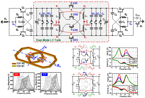
Figure 2. The SiGe HBT mode-switching hybrid class B/C VCO schematic and its operating principles.
A cryo-CMOS VCO using the same structure was also fabricated for comparison. The VCOs were measured at room temperature (296 K) and cryogenic temperature (3.5 K). At 3.5 K, the HBT VCO shows a 13.9 to 18.1 GHz tuning range and -141.7~-133.6 dBc/Hz phase noise at 10 MHz offset frequency while only consuming ~3 mW power. A 201.1 dBc/Hz of the best figure of metric is achieved. The flicker noise corner at cryogenic temperature is always below 650 kHz, which is much lower than the cryogenic CMOS VCO. It is believed this is the first reported SiGe HBT VCO designed for cryogenic applications.
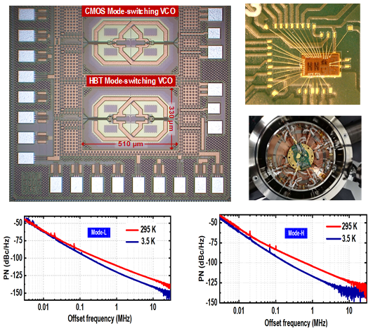
Figure 3. Micrograph of the chip fabricated in IHP 130nm SiGe BiCMOS technology, the PCB for cryogenic measurement, and the PN measured results.
The design described in this paper provides a reference for the research and development of cryogenic signal sources and cryogenic SiGe HBT chips for quantum applications. It provides new ideas to extend the VCOs’ frequency tuning range, overcome the start-up of class C oscillators, and reduce VCOs’ phase noise.
Prof. Yatao Peng from SIQSE at SUSTech is this paper’s first and corresponding author. SUSTech is the first unit of the paper.
Paper link: https://ieeexplore.ieee.org/document/9731542
To read all stories about SUSTech science, subscribe to the monthly SUSTech Newsletter.
Proofread ByAdrian Cremin, Yingying XIA
Photo By


