Professor Quan Pan’s team from the National Exemplary School of Microelectronics of the College of Engineering at the Southern University of Science and Technology (SUSTech) has made significant progress in the field of high-performance communication chip design, with research results including a low-power ultra-wideband communication chip for 5G communication, a low-power injection-locked clock signal recovery circuit chip for high-speed wired communication and a high-speed optical communication chip.
The research results have been published in the IEEE Journal of Solid-State Circuits (JSSC), a top journal of the IEEE Solid-State Circuits Society, the IEEE Transactions on Circuits and Systems I: Regular Papers (TCAS-I), a top journal of the IEEE Circuit and System Society, and the cover article of the first issue of the high-level national journal, Journal of Semiconductors (JOS). JSSC and TCAS-I are the top academic journals representing the highest international academic standards in the chip field.
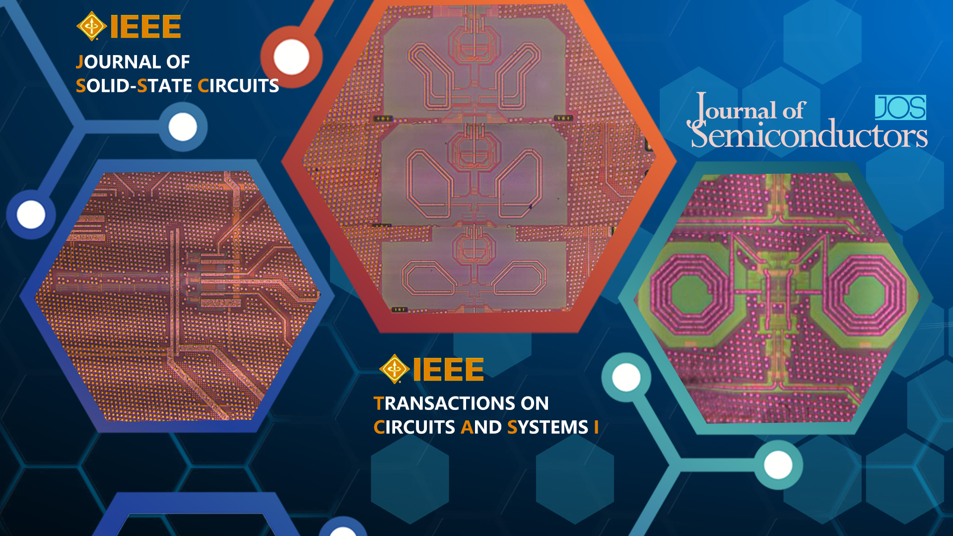
5G Communication Low-power Ultra-broadband Communication Chip
In recent years, mobile communications are ushering in a whole new era thanks to the accelerated pace of 5G commercialization and further research into millimeter wave technology. Currently, the division of frequency bands for 5G communications varies from country to country around the world. In addition to those already licensed, several unlicensed frequency bands need to be developed urgently.
For 5G millimeter-wave communication systems, ultra-broadband and low power consumption have always been important metrics. None of the world’s published millimeter-wave ILFDs can simultaneously cover all 5G licensed and unlicensed frequency bands. Therefore, an ultra-wideband injection-locked divider that can simultaneously support all frequency bands worldwide is essential.
The paper, entitled “Analysis and Design of Tuning-Less mm-Wave Injection-Locked Frequency Dividers with Wide Locking Range Using 8th-Order Transformer-Based Resonator in 40 nm CMOS,” was published in JSSC. It achieves the world’s widest locking range and highest energy efficiency ratio, covering all 5G millimeter-wave bands worldwide, and provides a feasible solution for designing injection-locked frequency dividers in the millimeter-wave field. The overall performance reaches a world-leading level, providing a feasible solution for the design of injection-locked frequency dividers in the millimeter-wave domain, which has practical implications for high-frequency multi-band applications in 5G communications.
It is worth mentioning that the team has deliberately designed the chip layout in the shape of three flowers without affecting the circuit’s performance. It is anticipated that SUSTech will have more independent and high-quality research results in the chip field in the future.

Figure 1. Micrographs of the three chips in paper
Jiang Qiyao, a research assistant in the School of Microelectronics at SUSTech, is the first author of this paper. Prof. Quan Pan is the sole corresponding author, and SUSTech is the sole institution for the paper.
Clock and Data Recovery Chip
In the rapid development of high-speed communication integrated circuits, to ensure the broad and reliable bandwidth, clock and data recovery (CDR), as the basic module of the communication system, is pivotal in the industrial production.
Wenbo Xiao, a master’s student in the School of Microelectronics and Prof. Pan’s group, alongside Qiwei Huang, and Hamed Mosalam, two postdoctoral researchers, have successfully designed and verified a low-power injection-locked oscillator-type clock and data recovery (ILCDR) in 40 nm CMOS. Their research, entitled “A 6.15–10.9 Gb/s 0.58 pJ/Bit Reference-Less Half-Rate Clock and Data Recovery With “Phase Reset” Scheme,” was published in TCAS-I.
In this paper, a novel “phase reset” scheme to periodically realign the clock phase to the rising edge of the data was proposed. In addition, a bang-bang phase detector (BBPD) compared the rising edge of the data and the clock after the phase alignment to achieve frequency capture. Moreover, the proposed structure utilizes a two-stage ring digitally controlled oscillator (DCO) instead of a four-stage ring DCO to further reduce the power consumption. Furthermore, based on the adopted structure, the proposed CDR significantly enhances the power efficiency compared to the previously reported CDRs. The measured capture range of the proposed CDR is 6.15 to 10.9 Gb/s, while consuming 5.8 mW from a 0.9 V supply voltage at 10 Gb/s. Energy efficiency of 0.58pJ/bit is successfully demonstrated, which reaches the highest international level of the same type of circuit.
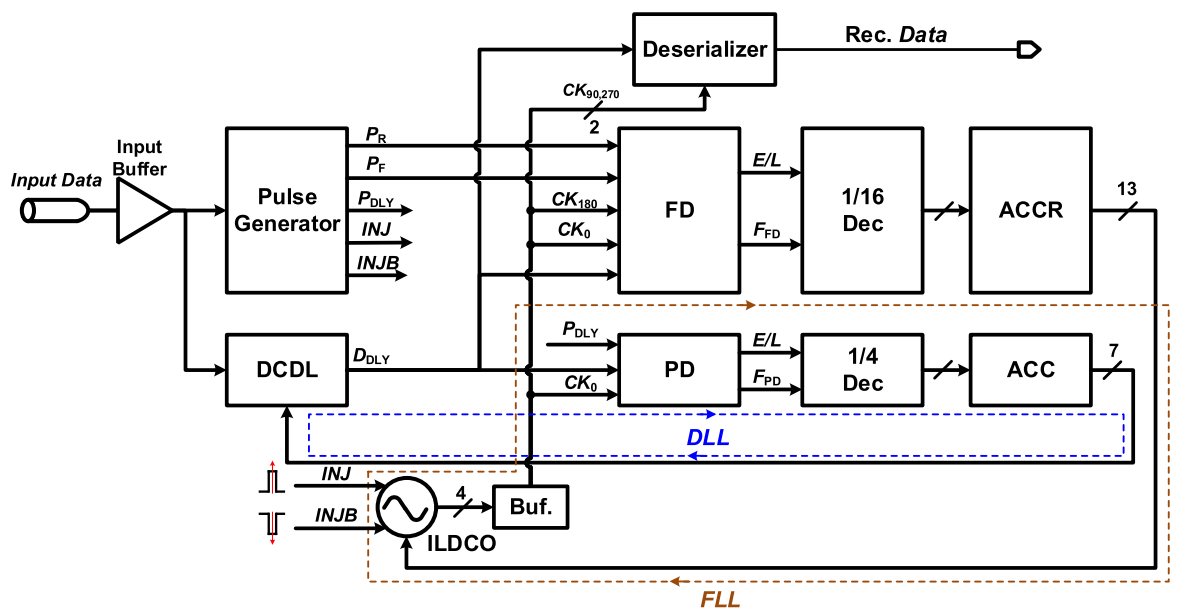
Figure 2. Architecture of proposed CDR circuit
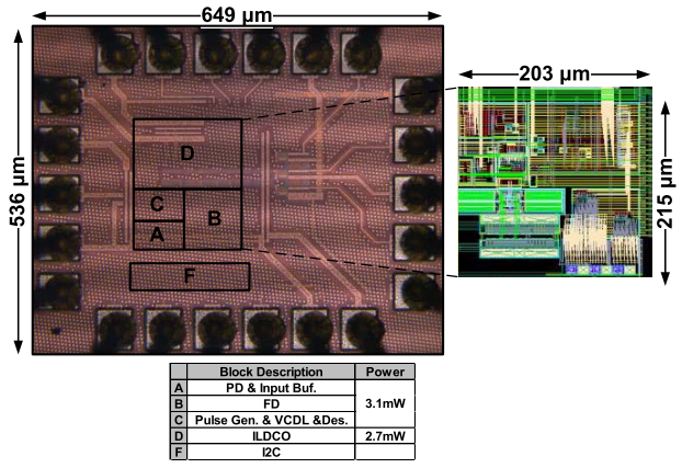
Figure 3. Die micrograph and power breakdown
Wenbo Xiao and Qiwei Huang are the co-first authors of this paper. Prof. Quan Pan is the sole corresponding author, and SUSTech is the sole unit of the paper.
High-speed optical communications
With the continually growing demand for multimedia applications and cloud computing, the promotion of high-speed communication is becoming more and more urgent. Compared with copper-based links, the optical interconnection is a more cost-effective and reasonable solution due to its excellent stability, high power efficiency, low cost, and broadband superiorities.
Transimpedance amplifier (TIA) is the most critical block in a typical optical communication receiver, and the biggest challenge of the TIA design comes from the large parasitic capacitance of the photodetector (PD), which limits both bandwidth and noise performance.
In this paper, entitled “A 58-dBΩ 20-Gb/s inverter-based cascode transimpedance amplifier for optical communications,” was published in JOS. Prof. Pan’s team proposes an inductive-peaking inverter-based cascode TIA to obtain high voltage gain and achieve better noise performance than its conventional inverter-based alternative. Series inductive peaking and negative capacitance techniques are also employed to further boost the bandwidth. The proposed TIA is fabricated in the TSMC 65-nm CMOS process. The measurement results show that this TIA can achieve a gain of 58 dBΩ up to 12.7-GHz bandwidth and 20-Gb/s clear data rate, while the power consumption is only 4 mW, the FoM is up to 454.
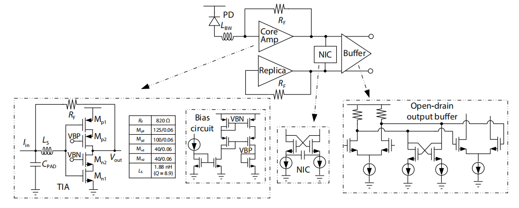
Figure 4. Schematic of the proposed TIA
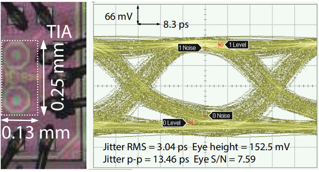
Figure 5. Chip micrograph & test results (eye diagram at 20Gb/s)
Luo Xiongshi, a master’s student in the School of Microelectronics at SUSTech, is the first author of this paper. Prof. Quan Pan is the corresponding author, and SUSTech is the only unit of the paper.
The research studies noted above were supported by the National Natural Science Foundation of China (NSFC), the Natural Science Foundation of Guangdong Province, and the Shenzhen Development and Reform Commission project.
Prof. Quan Pan’s research group welcomes outstanding undergraduates, graduate students, and postdoctoral fellows to join their team.
Paper links (In order of appearance above):
Q. Jiang and Q. Pan, “Analysis and Design of Tuning-Less mm-Wave Injection-Locked Frequency Dividers with Wide Locking Range Using 8th-Order Transformer-Based Resonator in 40 nm CMOS,” in IEEE Journal of Solid-State Circuits (JSSC), Mar. 2022.
https://ieeexplore.ieee.org/document/9728743
W. Xiao, Q. Huang, H. Mosalam, C. Zhan, Z. Li and Q. Pan, “A 6.15–10.9 Gb/s 0.58 pJ/Bit Reference-Less Half-Rate Clock and Data Recovery With “Phase Reset” Scheme,” in IEEE Transactions on Circuits and Systems I: Regular Papers (TCAS-I), vol. 69, no. 2, pp. 634-644, Feb. 2022.
https://ieeexplore.ieee.org/document/9585315
Q. Pan, X. Luo, “A 58-dBΩ 20-Gb/s inverter-based cascode transimpedance amplifier for optical communications,” in Journal of Semiconductors (JOS), Jan. 2022.
http://www.jos.ac.cn/article/doi/10.1088/1674-4926/43/1/012401
To read all stories about SUSTech science, subscribe to the monthly SUSTech Newsletter.
Proofread ByAdrian Cremin, Yingying XIA
Photo By