In traditional material systems, solid-state phase transitions typically refer to structural or property changes in response to external stimuli such as temperature, pressure, or chemical interaction. These transitions usually proceed continuously, with lattice reconstruction occurring simultaneously with energy input—such as in the cases of ion intercalation or atomic diffusion. However, previous studies observed an unusual palladium (Pd) diffusion-induced phase transition in palladium diselenide (PdSe2) under mild annealing, suggesting a previously unknown, non-classical thermodynamic pathway.
A research team led by Professor Junhao Lin from the Department of Physics at the Southern University of Science and Technology (SUSTech) has made significant advances in understanding phase transition mechanisms in two-dimensional (2D) materials. For the first time, the team has revealed a previously unreported latent phase transition behavior in 2D PdSe2, a phenomenon that deviates fundamentally from conventional solid-state phase transitions.
Their study, titled “Latent phase transition in 2D PdSe2,” has been published in Physical Review Letters, one of the most prestigious journals in physics, and was selected as an Editor’s Suggestion—a recognition awarded to only a small fraction of papers to highlight particularly important or impactful work.
Building on earlier collaborative work with Professor Feng Miao’s team at Nanjing University (Nature Materials 23, 1363, 2024), the researchers leveraged a self-developed on-chip phase engineering platform and employed in-situ aberration-corrected transmission electron microscopy (STEM) to investigate the structural evolution of PdSe2 at atomic resolution. They uncovered, for the first time, a latent phase transition mechanism in 2D materials. Unlike conventional continuous or abrupt transitions, this transformation occurs under continuous energy input but retains structural stability for an extended period. Only when internal chemical pressure reaches a critical threshold does the lattice abruptly collapse into a three-dimensional Pd17Se15 phase.
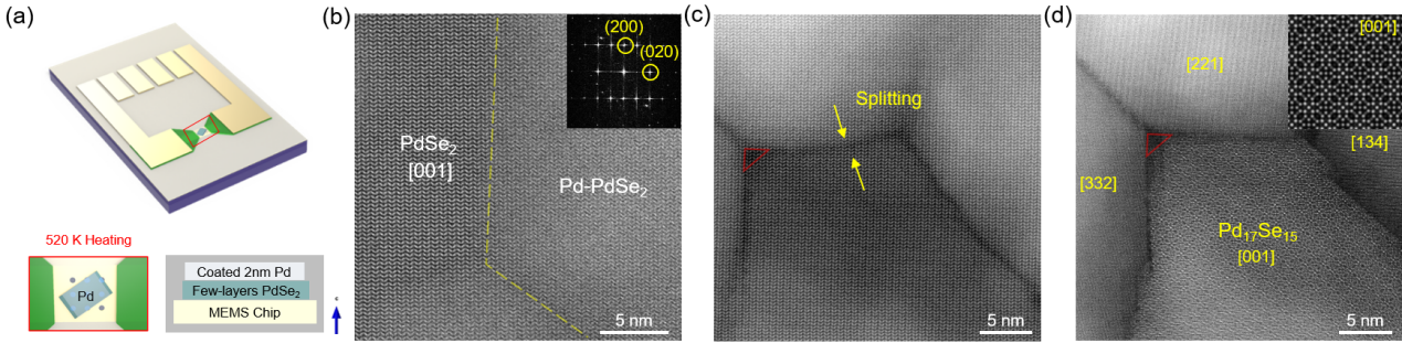
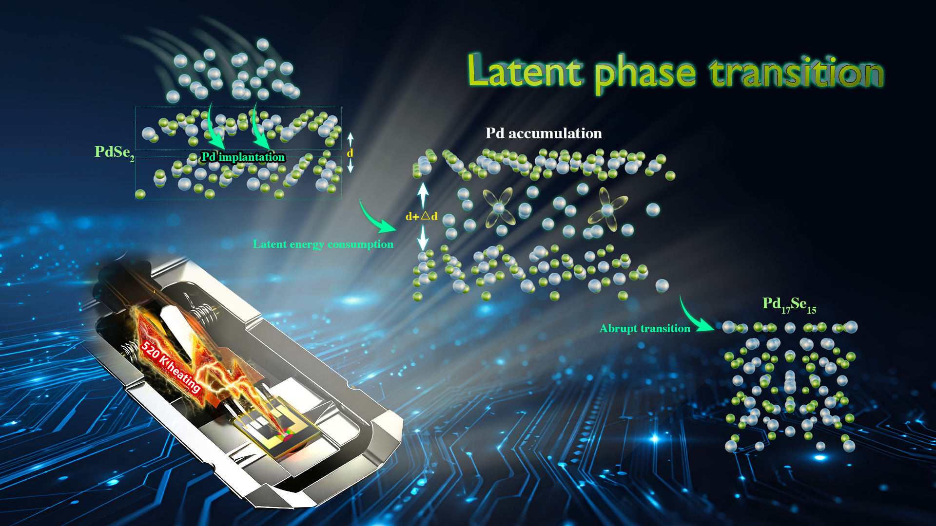
Figure 1. On-chip phase engineering and latent phase transition behavior in PdSe2
Based on the group’s independently developed techniques for precision transfer and stacking of 2D materials (national invention patents CN114486960A and CN114361021A), this study achieves damage-free transfer of ultrathin 2D materials onto fragile MEMS chips and enables controllable electrical–thermal dual-field modulation during in-situ electron microscopy characterization (Nature Communications, 15, 6074, 2024).
In the experiment, a ~2 nm thick Pd layer was thermally evaporated onto the PdSe2 surface, followed by in-situ annealing at a mild temperature of ~250 °C. Using a glovebox-integrated in-situ STEM platform, the team conducted atomic-resolution, real-time tracking of the structural evolution of PdSe2 under Pd injection and heating.
Tracking of electron diffraction intensities further revealed the dynamics of a threshold-triggered process: the diffraction peaks of PdSe2 remained stable for an extended period before rapidly diminishing at a critical moment, while the characteristic peaks of Pd17Se15 surged abruptly. This behavior exhibits a classic three-stage kinetic process—latent accumulation, threshold-triggered collapse, and grain integration.
Further analysis showed that surface Pd atoms gradually diffuse into the van der Waals (vdW) gaps and continue to accumulate. Despite ongoing energy absorption, the PdSe2 lattice remains structurally intact for a prolonged time, even showing cracking due to vertical expansion while retaining the 2D layer structure. Once the internal chemical pressure reaches a critical threshold, however, the lattice abruptly collapses into the 3D crystalline phase Pd17Se15. This “energy storage – threshold activation – instantaneous transition” process clearly reflects the fundamental characteristics of a latent phase transition.
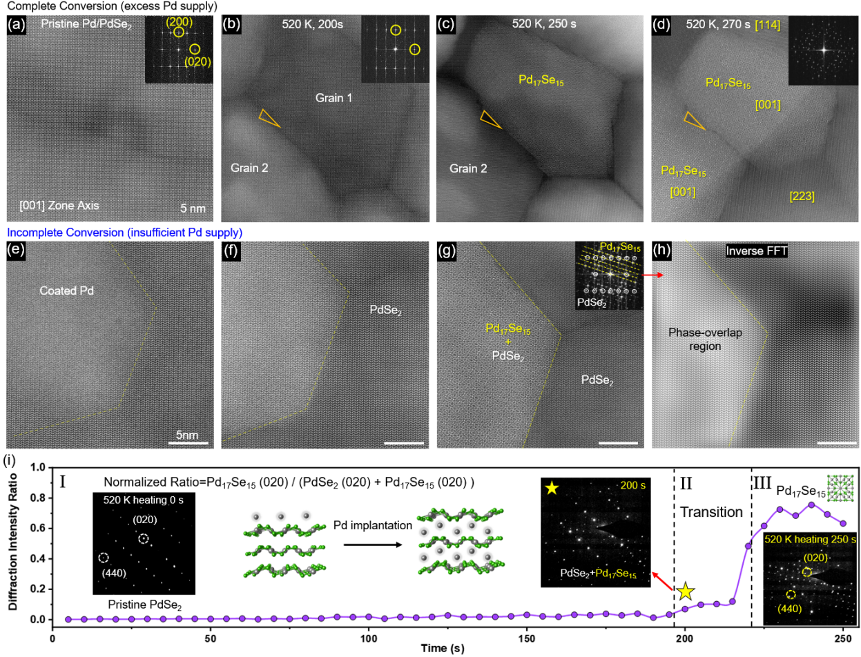
Figure 2. Atomic-scale characterization of the phase transition process
Using first-principles calculations and ab initio molecular dynamics simulations, the team further uncovered the microscopic mechanism underlying the latent phase transition. The results show that the diffusion barrier for Pd atoms entering the interlayer space of PdSe2 from the surface is approximately 0.69 eV, and an energy well of about –0.45 eV exists within the vdW gap, which facilitates Pd trapping and sustained interlayer accumulation. The energy barrier for further vertical diffusion into deeper layers is around 0.49 eV, indicating considerable vertical migration capability within the system.
In contrast to conventional layered materials such as MoSe2 or TiSe2, the Pd–Pd and Pd–Se bond energies in PdSe2 are among the weakest within the transition metal chalcogenides. These exceptionally weak interactions allow the crystal lattice to maintain its structural integrity during the Pd migration process.
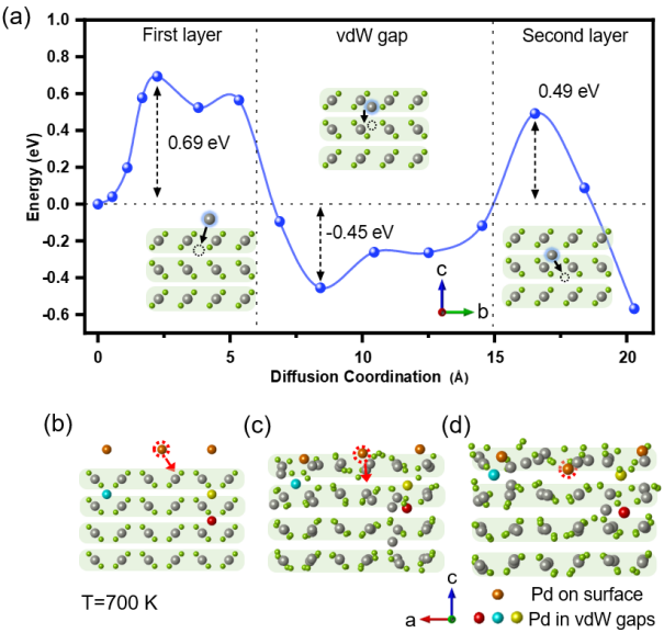
Figure 3. Low migration barrier and molecular dynamics simulation of Pd diffusion
Further simulations of gradual Pd atom injection into the vdW gaps revealed that while the in-plane lattice constants remained nearly unchanged, the interlayer spacing increased significantly with Pd content, indicating the continuous accumulation of Pd atoms between the layers. Energy analysis identified two competing effects induced by Pd intercalation: interlayer expansion, which increases the system’s energy (ΔEvdW), and Pd–lattice interactions, which lower the energy (ΔEimp).
In the early stages, the system’s energy increases, indicating that PdSe₂ resists intercalation. However, once the Pd concentration exceeds a critical threshold, ΔEimp becomes dominant, causing a sharp drop in energy and triggering a structural transformation. In contrast to conventional ion intercalation processes—such as Li insertion in MoSe₂—that show a monotonic energy decrease and a continuous phase transition, the phase transition in PdSe₂ exhibits pronounced “delay” and “threshold-triggered” characteristics.
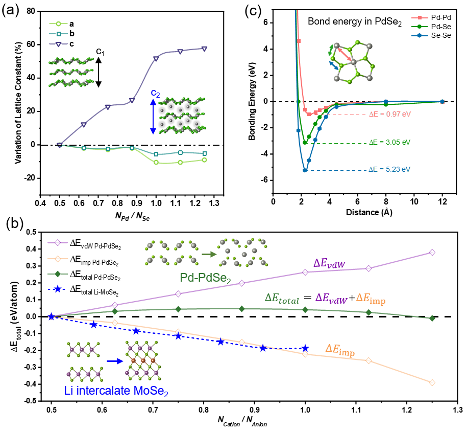
Figure 4. Investigating the mechanism of latent phase transition triggered by Pd implantation
This mechanism resembles the process of latent heat absorption during water vaporization: the absorbed heat weakens hydrogen bonding while the overall temperature remains constant. In the initial stage of the PdSe2 phase transition, the 2D atomic layer structure remains intact, and the thermal energy absorbed by the system is used to weaken the interlayer vdW interactions. Once the Pd concentration surpasses a critical threshold, the 2D PdSe2 framework abruptly collapses into the 3D Pd17Se15 phase—closely analogous to water undergoing vaporization. This discovery not only unveils an unprecedented mode of structural transformation in PdSe2 but also offers a new perspective for understanding solid-state phase transitions in 2D materials.
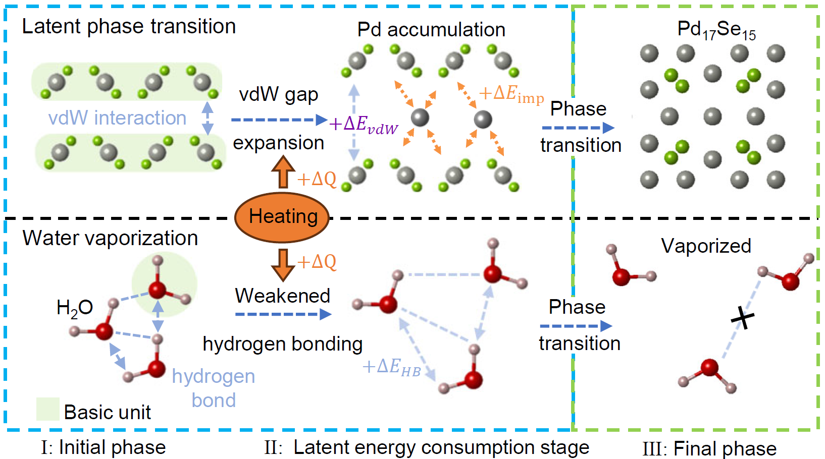
Figure 5. Analogy between the latent phase transition and the latent heat–driven vaporization of water
Building on this discovery, the team further applied the phase transition mechanism to device fabrication. By depositing ~30 nm thick Pd electrodes onto the PdSe2 surface, in-situ STEM observations revealed that Pd17Se15 grains grew laterally by gradually consuming the underlying PdSe2. This strategy offers a novel approach for constructing high-quality 2D metal–semiconductor contacts under mild thermal conditions.
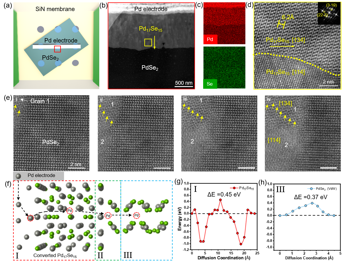
Figure 6. Pd-induced phase transition via lateral migration
This study introduces and experimentally verifies the concept of a “latent phase transition” in 2D material systems for the first time. This mechanism illustrates a universal principle whereby a system can undergo prolonged energy accumulation without structural transformation under external stimuli, until a critical threshold of internal chemical pressure is reached, triggering an abrupt structural collapse. This discovery deepens our understanding of phase transition dynamics in low-dimensional materials and offers a novel theoretical and experimental framework for designing 2D–3D heterostructures, enabling low-temperature phase engineering, and fabricating highly stable functional devices.
Postdoctoral researcher Qishuo Yang from the Department of Physics at SUSTech, Research Assistant Professor Yabei Wu from the Department of Materials Science and Engineering (MSE) at SUSTech, and Dr. Liang Zhu, formerly a postdoctoral fellow at SUSTech, are co-first authors of the paper. Professor Junhao Lin and Chair Professor Wenqing Zhang from the Department of MSE are the corresponding authors.
Other contributing teams to this work include Professor Feng Miao’s group at Nanjing University, Professor Zhigang Chen’s group at Queensland University of Technology, and Professor Jin Zou’s group at the University of Queensland.
Paper link: https://doi.org/10.1103/hcy1-7znw
To read all stories about SUSTech science, subscribe to the monthly SUSTech Newsletter.
Proofread ByAdrian Cremin, Yuwen ZENG
Photo ByYan QIU


