A group of researchers at Southern University of Science and Technology (SUSTech) have further improved aluminum gallium nitride (AlGaN) and gallium nitride (GaN) high electron mobility transistor (HEMT) devices through the use of novel process technologies and materials.
School of Microelectronics Professor Yu Hongyu has led his research teams to publish papers in high-impact journals in the field of electronic devices, specifically IEEE Electron Device Letters, IEEE Transactions on Electron Devices and IOP Semiconductor Science and Technology.
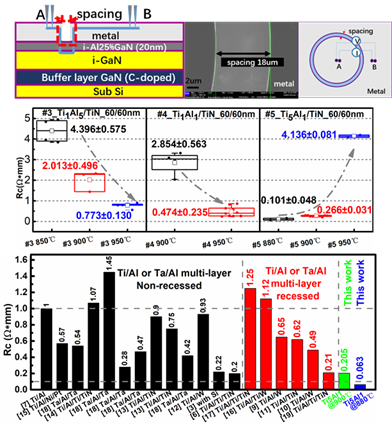
The paper published in IEEE Electron Device Letters (IF = 3.753) was titled “Ultra-Low Contact Resistivity of < 0.1 Ω⋅ mm for Au-Free TixAly Alloy Contact on Non-Recessed i-AlGaN/GaN.” The article was deemed to be a significant contribution to the field and, as such, was selected as the cover article for the issue.
AlGaN/GaN HEMT devices are highly attractive for radio frequency and power switching devices. These HEMT devices have a lower resistance, which affects the performance parameters of the device.
Typically, metal stacks within HEMT devices are made up of titanium, aluminum, nickel, and gold (Ti/Al/Ni/Au), while others have incorporated substances like molybdenum (Mo). The research led by Professor Yu Hongyu proposed a new contact metal material with a low resistance base that does not require recess-etching.

Electrical characteristics of ohmic contact in AlGaN / GaN TixAly alloy
The research team proposed the use of a TixAly alloy layer as the direct contact. The team’s testing set a new world record of 0.063 Ω· mm for ohmic contact resistance using TiAl alloy. Further analysis found that the extraction of titanium on nitrogen had a significant impact on the final ohmic characteristics, opening up a new direction for gold-free ohmic contacts. A patent has been applied for by the team.
Fan Mengya, a visiting student of the SUSTech School of Microelectronics (originally from the Fudan University School of Microelectronics), was the first author of the paper.
Paper link: https://ieeexplore.ieee.org/document/8897034
The paper published in IEEE Transactions on Electron Devices (IF = 2.704) was titled “Gate Leakage Suppression and Breakdown Voltage Enhancement in p-GaN HEMTs Using Metal/Graphene Gates.”
The most promising commercial direction for HEMT power devices is p-GaN gate HEMT device structures. However, there are several challenges associated with these structures that need to be solved before their implementation on a commercial scale. To this end, there has been considerable research into the use of graphene in semiconductors, and its use in GaN devices. Such research is currently in its early stages, and research groups around the world are still learning a considerable amount.
Professor Yu Hongyu and his team hypothesized that applying graphene to a p-GaN gate HEMT device would reduce gate leakage current, and increase gate breakdown voltage, thereby solving the existing gate reliability problems.

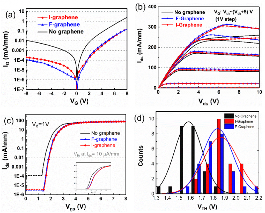
Comparison of electrical characteristics of p-GaN gate HEMT devices with and without graphene
The team found that by adding graphene, gate leakage reduced by a magnitude of fifty, and threshold voltage could also increase. Other indicators also improved. A physical analysis determined that graphene effectively reduced the reaction between metals and p-GaN. The team also found that the reduced gate leakage and increased gate breakdown voltage makes the introduction of graphene to a p-GaN gate HEMT device more commercially viable than previous devices.
Zhou Guangnan, a student of the SUSTech School of Microelectronics, was the first author of this paper.
Paper link: https://ieeexplore.ieee.org/document/8995788
The third paper, “Increasing Threshold Voltage and Reducing Leakage of AlGaN/GaN HEMTs Using Dual-Layer SiNx Stressors,” was published in IOP Semiconductor Science and Technology (IF = 2.654).
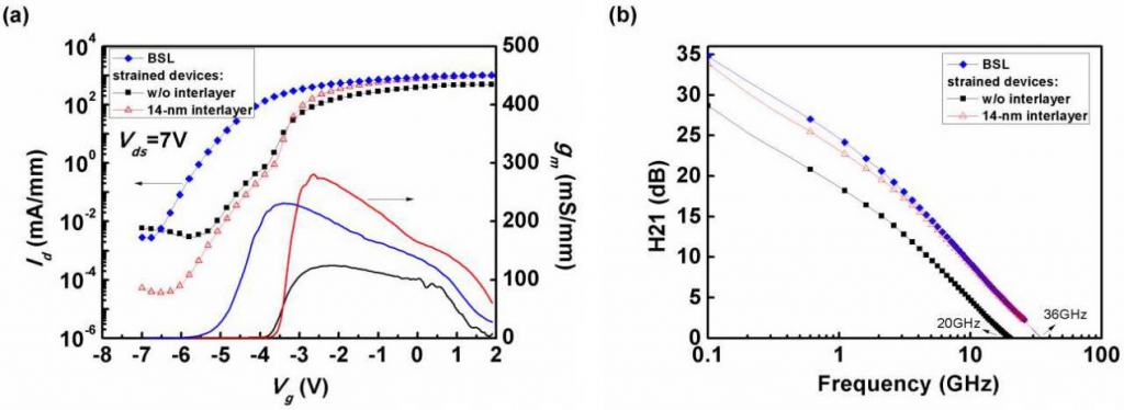
The current etching process of the semiconductor layer of normally-off AlGaN/GaN HEMT devices tend to introduce defects into the device, thereby reducing its reliability, which is the reason it has rarely been commercialized.

The research group proposed taking advantage of the piezoelectric properties of GaN to modulate the HEMT. They applied a high-stress silicon nitride (SiN) film to the gate area and were able to increase the device’s threshold voltage by 1V. The use of a unique double-layer SiN film that protects the semiconductor surface does not inhibit any of the other properties of the device, and as such, a patent has been applied for this new technology. They also found that voltage stress can suppress reverse bias, which is potentially a new way to modulate AlGaN / GaN HEMT devices.
Cheng Wei-Chih, a joint-trained doctoral candidate of SUSTech and the Hong Kong University of Science and Technology (HKUST), is the first author of this paper.
Paper link: https://iopscience.iop.org/article/10.1088/1361-6641/ab73ea
The team thanked the SUSTech Core Research Facilities (SCRF, formerly the Materials Characterization and Preparation Center – MCPC).
Proofread ByXia Yingying
Photo BySchool of Microelectronics, Qiu Yan