Along with the miniaturization and integration of products in fields of optics and electronics, ultrafast laser nanofabrication has attracted significant attention due to its merits like high precision, excellent freedom, and low material damage. However, laser nanofabrication methods capable of breaking the diffraction limit with high efficiency are still a long-pending challenge to overcome and require further exploitation.
Assistant Professor Shaolin Xu’s team from the Department of Mechanical and Energy Engineering at the Southern University of Science and Technology (SUSTech) has recently made significant progress in the field of high-resolution ultrafast laser nanofabrication.
Their studies have been published in high-level journals on laser micro-/nanomanufacturing, including Nature Communications, Advanced Optical Materials, Laser & Photonics Reviews, Nano Letters, and ACS Applied Materials & Interfaces. Their works contained laser subwavelength nanopatterning, laser-induced periodic nanogratings, line-shaped laser lithography for heterarchical micro-/nanofabrication, and laser-doping enhanced plasma etching of robust nanocones.
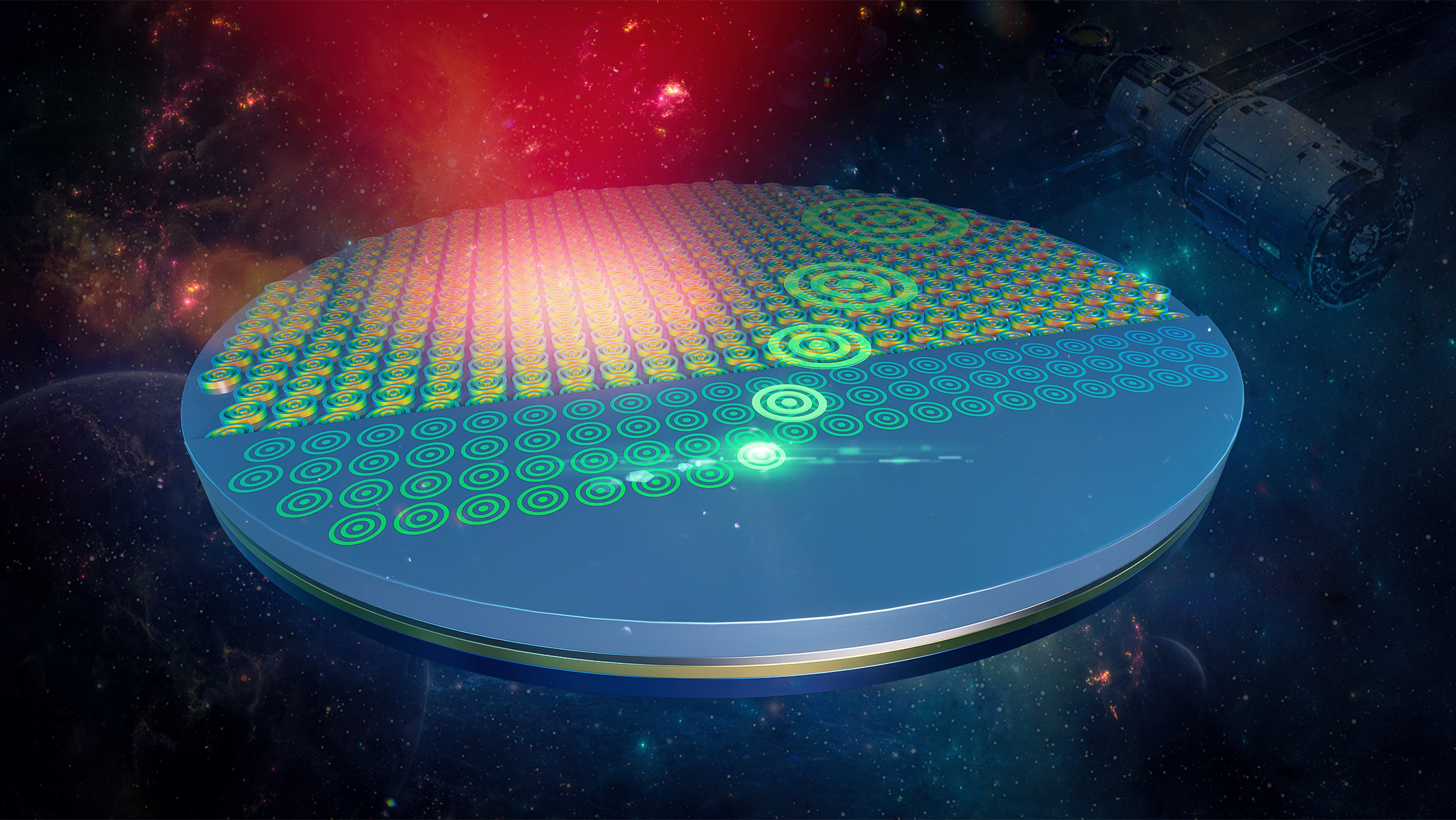
Subwavelength patterned pulse laser lithography
Large-area seamless patterned nanofabrication beyond diffraction limit plays a crucial role in manufacturing semiconductors and optical micro-nano devices. It is pretty meaningful to develop low-cost and high-efficient processing technology with related equipment for the breakthrough of micro-nano manufacturing.
The researchers created ultrafast laser pulses with sub-wavelength patterned wavefronts by modulating the beam polarization with quasi-binary phase masks. The pulse separation from fast scanning was applied to form periodic modification/ablation, efficiently realizing uniform wafer-level surface patterned micro-nano structures in the atmospheric environment. The seamless patterned structure is highly controllable in shape and has a sub-wavelength resolution (around 300 nm with a laser of 520 nm wavelength). In addition, they designed and fabricated meta-absorbers to achieve unimodal and bimodal absorption rates up to 98% in the mid-infrared wavelength (3-7 μm). This efficient laser subwavelength patterning processing method is generally applicable to the patterning of any thin film material.
These results were published in Nature Communications, entitled “Sub-wavelength patterned pulse laser lithography for efficient fabrication of large-area metasurfaces”, and Advanced Optical Materials, entitled “Large-Scale Laser Nanopatterning of Multiband Tunable Mid-Infrared Metasurface Absorber”.
Doctoral students Lingyu Huang and Kang Xu are the co-first authors of the Nature Communications paper. Dandan is the first author of the Advanced Optical Materials article. Prof. Shaolin Xu is the corresponding author, and SUSTech is the first corresponding unit for both papers.
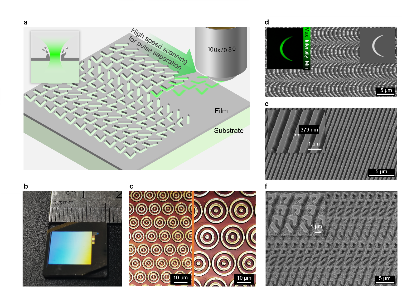
Figure 1. Subwavelength patterned pulse laser lithography
Laser-induced periodic nanograting manufacturing
Laser-induced periodic surface structure (LIPSS) can break through the diffraction limit of light and form nanogratings with subwavelength (~λ/2) to ultra-deep subwavelength (~λ/8) resolution. However, the native structural disorder limits its practical applications.
For the first time, based on the study of the ultrafast-laser-induced surface plasmon wave interference phenomenon, Prof. Xu’s team systematically explained the origin of laser-induced structure disorder of nanogratings with the newly proposed self-alignment phenomenon. Utilizing this phenomenon, they realized the efficient large-area processing of long-range ordered sub-wavelength gratings. Furthermore, the wafer-level uniform 2D nanostructures were achieved by spontaneously forming the ordered nanogratings mentioned above, which came from a uniform line-shaped ultrafast laser ablation by adjusting the proper scanning strategy.
The above research work was published in Laser & Photonics Reviews, entitled “Self-Aligned Laser‐Induced Periodic Surface Structures for Large‐Area Controllable Nanopatterning”, and Nano Letters, entitled “Self-Aligned Plasmonic Lithography for Maskless Fabrication of Large-Area Long-Range Ordered 2D Nanostructures”.
Doctoral students Jiaxu Huang and Kang Xu are the co-first authors of the Laser & Photonics Reviews paper. Jiaxu Huang is the first author of the Nano letters publication. Prof. Shaolin Xu is the corresponding author, and SUSTech is the first corresponding unit for both papers. Doctoral student Jun Li also contributed to these works.
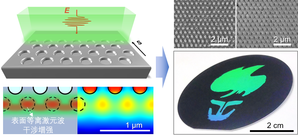
Figure 2. Self-aligned laser-induced periodic 2D nanogratings
Line-shaped laser lithography for heterarchical micro-/nanofabrication
Metal micro-/nanogrids across large scales (sub-100-nm to several micrometers scales) can effectively improve the light transmission, conductivity, and mechanical stability of transparent flexible electronic devices. However, these heterarchical micro-/nanostructures’ efficient and affordable processing is still extremely challenging.
The researchers proposed a one-step maskless line-shaped laser lithography technique to efficiently produce continuously controllable metal grids, whose linewidths are tunable from 50 nm to several micrometers, by modulating the separated ablation of line-shaped laser pulses. They utilized this technology to fabricate a flexible transparent electrode, which had a thin layer resistance of 4.6 Ω/sq under the premise of high transmittance of up to 80%. The good photoelectric performance was still maintained after 1,000 times of bending tests. Furthermore, they designed and manufactured a robust, flexible multidirectional strain sensor with advanced sensitivity and responsiveness, which realized the function of multidirectional strain sensing by using a single layer of the structured thin film.
These results were published in ACS Applied Materials & Interfaces, entitled “Laser-patterned hierarchical aligned micro-/nanowire network for highly sensitive multidimensional strain sensor”, and Advanced Materials Technologies, entitled “Line-shaped laser lithography for efficiently fabricating flexible transparent electrodes with hierarchical metal grids across λ/10 to microscale”.
Master’s student Liang Zhao is the first author of the ACS Applied Materials & Interfaces paper. Jingyu Qiao is the first author of the Advanced Materials Technologies article. Prof. Shaolin Xu is the corresponding author, and SUSTech is the first corresponding unit for both papers.
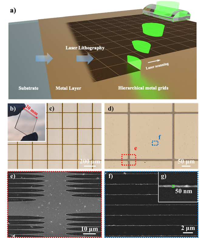
Figure 3. Line-shaped laser lithography for heterarchical micro-/nanofabrication
Laser-doping enhanced plasma etching of robust nanocones
Surface nanostructures can effectively reduce Fresnel reflection at the interface, thereby improving the transmissivity of optical windows. However, surface structures such as nanocones are prone to wear and fracture when subjected to friction or particle impact, which results in performance failure, and limits their application in extreme environments.
Prof. Xu’s team designed a micro-frame structure to protect the surface nanocone array, offering high wear resistance to the anti-reflective surface. Combining ultrafast laser processing and dry etching, they proposed a locally laser-doping enhanced dry etching technology, which supported the manufacturing of optical anti-reflection windows with high transmittance and excellent robustness on quartz glass and intrinsic SiC. The proposed design and manufacturing method is expected to promote the research and application of optical anti-reflection windows in extreme environments.
The results were published in ACS Applied Materials & Interfaces, entitled “Armored Nanocones Engraved by Selective Laser Doping Enhanced Plasma Etching for Robust Supertransmissivity”.
Doctoral students Kang Xu and Jin Hu are the co-first authors of this paper. Prof. Shaolin Xu is the corresponding author, and SUSTech is the first corresponding unit.
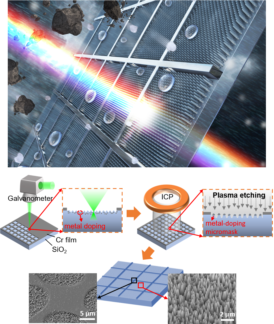
Figure 4. Laser-doping enhanced plasma etching of robust nanocones
Other contributors to these studies from SUSTech included Prof. Wenqing Zhang, Prof. Qi-Huo Wei, Assoc. Prof. Yanjun Liu, and Asst. Prof. Min Wang.
Prof. Yongfeng Lu from the University of Nebraska-Lincoln, Prof. Gary J. Cheng from Purdue University, and Prof. Xinwei Wang from Iowa State University also provided valuable comments and suggestions for the development and publication of these papers.
The above research works were supported by the Science, Technology and Innovation Commission of Shenzhen Municipality, Shenzhen Guihua Intelligent Technology Co., Ltd., Huawei Technologies Co., Ltd., Guangdong Original Point Technology Co., Ltd., and SUSTech Core Research Facilities.
Paper links (In order of appearance above):
Nature Communications: https://www.nature.com/articles/s41467-022-33644-8
Advanced Optical Materials: https://onlinelibrary.wiley.com/doi/10.1002/adom.202200939
Laser & Photonics Reviews: https://onlinelibrary.wiley.com/doi/10.1002/lpor.202200093
Nano Letters: https://pubs.acs.org/doi/10.1021/acs.nanolett.2c01740
ACS Applied Materials & Interfaces: https://pubs.acs.org/doi/10.1021/acsami.2c14642
Advanced Materials Technologies: https://onlinelibrary.wiley.com/doi/10.1002/admt.202200125
ACS Applied Materials & Interfaces: https://pubs.acs.org/doi/10.1021/acsami.2c13033
To read all stories about SUSTech science, subscribe to the monthly SUSTech Newsletter.
Proofread ByAdrian Cremin, Yingying XIA
Photo By