Glasses are among the most important high-performance materials of the 21st century. Microstructured glass components have recently become increasingly significant in integrated optics, electronics, biofluidics, and other fields. This surge in importance can be attributed to their excellent characteristics, including high optical transparency, exceptional mechanical and chemical stability, and superior thermal and electrical insulation properties.
To leverage the potential of microstructured glass components, fabrication strategies must be scalable and capable of processing with high precision in terms of specific size, shape, and surface quality. Nevertheless, achieving these objectives proves challenging due to glass’s hard, brittle features and low heat conductivity, leading to chipping, cracking, and other stress damage.
Associate Professor Shaolin Xu’s research team from the Department of Mechanical and Energy Engineering (MEE) at the Southern University of Science and Technology (SUSTech) has recently made significant progress in ultrafast laser micro/nanofabrication. They have published two papers focusing on developing new ultrafast laser micromachining technologies by using beam shaping technology, including Bessel and cylindrical vector beams. Their breakthrough enables the fabrication of precision microstructures on the surfaces of glass and hybrid micro-nano structures on silicon carbide, providing new solutions for designing and fabricating various optical devices.
Their papers have been published in renowned journals, such as the International Journal of Machine Tools and Manufacture (IJMTM) and Advanced Functional Materials (AFM).
Revolutionary laser precision micromachining of glass
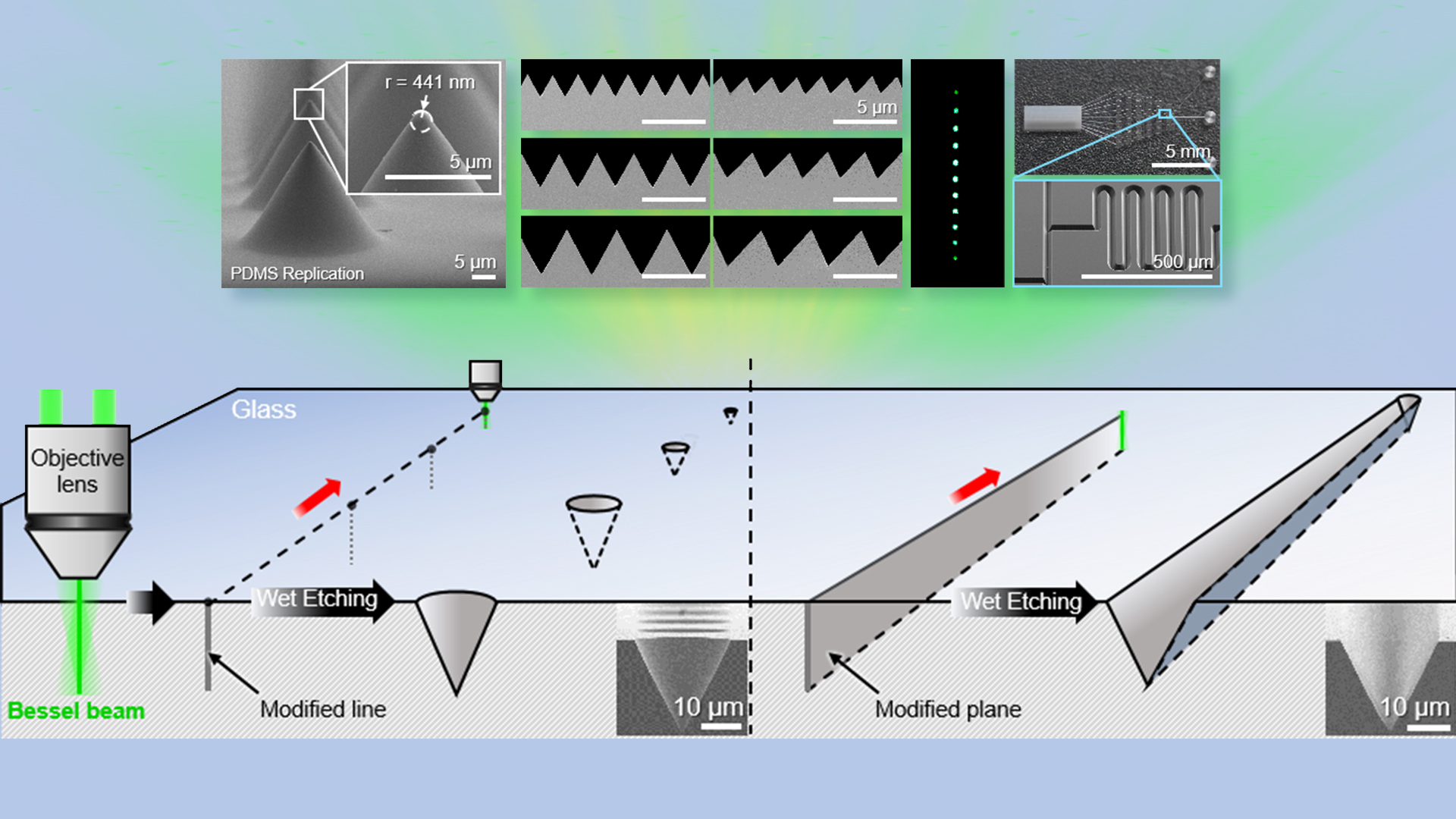
In their first paper, the group’s discovery of a new phenomenon, where laser-modified regions break the rule of inherently isotropic glass etching and regulate a directional anisotropic etching along modified tracks, has led to the development of a laser-guided anisotropic etching (LGAE) method (Figure 1). This method enables crafting precision glass microstructures with sharp features, smooth surfaces, and adjustable shapes and sizes.

Figure 1. Principle of laser-guided anisotropic etching (LGAE).
An ultrafast Bessel beam is utilized to create high aspect-ratio line-shaped modification within the glass. With a higher etching rate than pristine glass, the modified line guides directional anisotropic etching along the modified track, facilitating the formation of a V-shape with an angle altered by the etching ratio. These modified lines can further serve as basic building blocks to interconnect to construct a 3D internal modification region and then guide the glass’s overall surface morphology etching evolution, enabling the creation of microstructures featuring designable shapes and adjustable feature sizes.
To accurately predict and control the shape of the microstructures, the researchers establish a finite difference etching model that incorporates localized etching rate regulation, validating the robustness and controllability of LGAE. This scalable method has successfully fabricated a 50 μm period micro-pyramid array with high uniformity over a centimeter-scale area, demonstrating its suitability for large-scale manufacturing.
The showcased micro-engineered glass components encompass V-groove arrays for fiber alignment, blazed gratings for light modulation, and microchannels with customized trajectories for microfluidic chips, as shown in Figure 2. These advancements driven by LGAE can significantly contribute to the progress of glass-based research and industries.
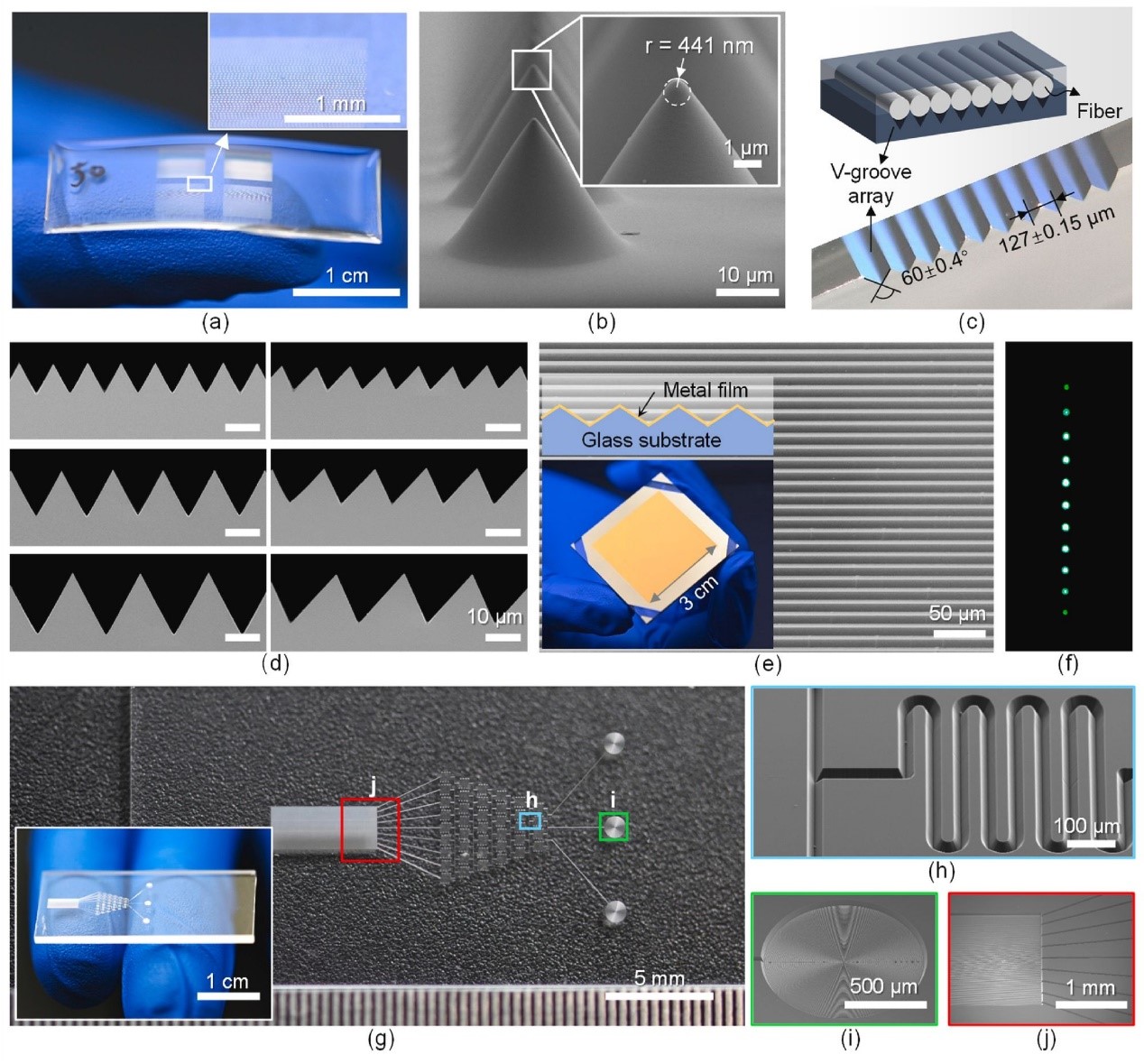
Figure 2. Applications of micro-engineered glass components fabricated by the LAGE method. (a-b) Micro-needles manufactured through PDMS replication; (c) V-groove arrays enable precise fiber placement and alignment; (d-e) Blazed grating; (g-j) Microfluidic system.
This work, entitled “Laser-guided anisotropic etching for precision machining of micro-engineered glass components”, has been published in the International Journal of Machine Tools and Manufacture.
Jun Li, a Ph.D. student from the Department of MEE at SUSTech, is the first author of this paper. Associate Professor Shaolin Xu from the Department of MEE at SUSTech is the corresponding author, and SUSTech is the primary affiliation. Other significant contributors to this study include Shuai Zhong, Jiaxu Huang, Pei Qiu, Pu Wang, Hui Li, and Duo Miao from Shaolin Xu’s team, as well as Chu Qin from the School of Microelectronics (SME) at SUSTech.
Unlocking ultra-broadband absorption with light-trapping SPhPs
In their second paper, the researchers present an engaging optical absorption mechanism called light-trapping-enhanced surface phonon polaritons (SPhPs) excitation effect to help realize an ultra-broadband absorber on 4H-type silicon carbide (4H-SiC) from visible to far-infrared wavelength.
Ultra-broadband perfect absorbers of electromagnetic waves have garnered significant interest in diverse applications such as radiation coolings, photovoltaics, electromagnetic shielding, imaging, sensing, and stealthing. While the homogeneous hierarchical structures combine surface structures of multiple scales and types that exhibit diverse light responses, it has the potential to facilitate ultra-broadband and wide-angle absorption.
Structures with feature sizes far larger than a wavelength, such as cones or pits, can confine the electromagnetic waves by light trapping. Sub-wavelength nanostructures reveal abnormal light response on account of equivalent gradient refractive index for dielectric or localized surface plasmon resonance for materials possessing metallic properties. Hierarchical structures can integrate the aforementioned effects by composing the above multi-scale structures, achieving better absorption performance (Figure 3).
4H-SiC is a highly desirable material for optoelectronic devices. It has great durability, containing excellent resistance to high working temperatures and stable chemical and physical properties. In the reststrahlen band of 4H-SiC, where intrinsic heavy reflection occurs, the SPhPs excited by metamaterials-like nanogratings on the surface can be enhanced by light trapping from the microcones (Figure 3), thereby improving absorption and resulting in non-intrinsic material properties to achieve perfect absorption. Outside the reststrahlen band, the light trapping effect dominates the antireflection causes, and the nanogratings serve as an equivalent antireflection layer to further improve bulk absorption.
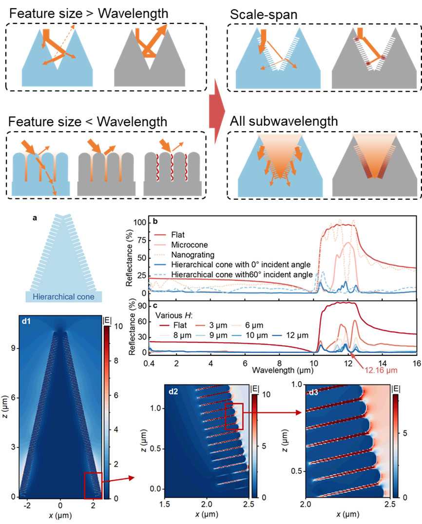
Figure 3. Design of hierarchical cone and the SPhPs excitation effect
Ultrafast laser fabrication has recently emerged as a promising strategy for the one-step processing of microstructures with engraved nanostructures. The cylindrical vector beams with designable polarization distributions have been considered to create hierarchical micro-nanostructures with nanogratings on the surface in a single step. The group introduces a one-step fabrication method to produce hierarchical cone arrays on doped 4H-SiC with engraved high aspect ratio nanogratings through ring-shaped vector beam multi pulses deposition.
The ring-shaped vector beam is generated by polarization modulation utilizing a half-wave plate (HWP), spatial light modulator (SLM), and a quarter-wave plate (QWP). The singularity at the beam center arises from the axial symmetry of polarization. It leads to the formation of the microcone structure, and the radial polarization leads to the generation of nanogratings during pulses deposition. As shown in Figure 4, the hierarchical cones exhibit exceptional broadband performance, achieving an average absorptance of 98% over the spectrum of 0.4-16 μm with wide-angle feasibility. Additionally, under infrared camera detection, the hierarchical cone arrays exhibit great absorption in the detectable wavelength range of 7.5-14 μm with an Au film background. Additionally, the microcone arrays show worse absorption than the hierarchical type.
Notably, the hierarchical cones can be applied to various materials, showing significant potential for use in photodetectors, and the proposed SPhPs excitation effect provides a new avenue in electromagnetic wave modulation.
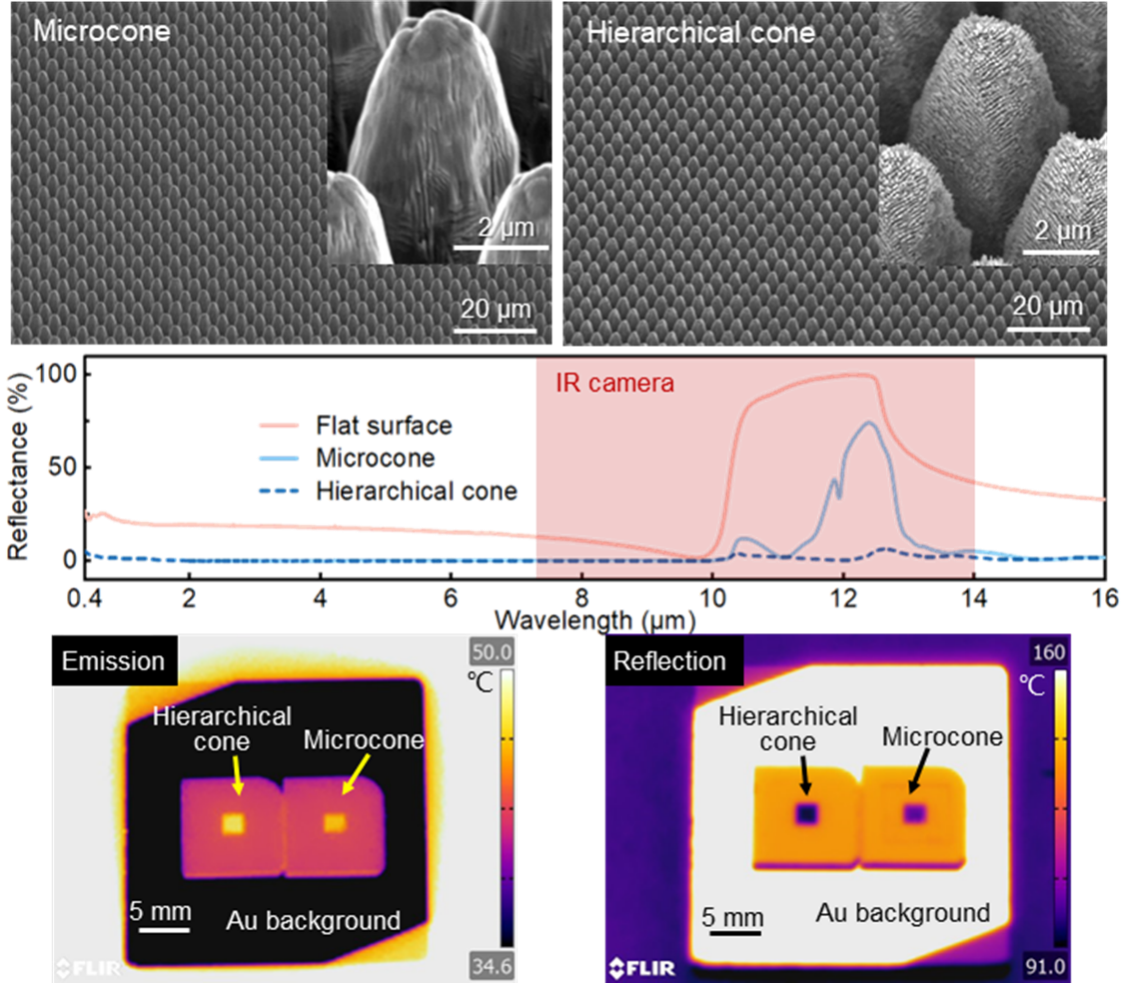
Figure 4. The reflectance of the absorber with its detailed surface morphology
The above work, entitled “Hierarchical Conical Metasurfaces as Ultra-broadband Perfect Absorbers from Visible to Far-Infrared Regime”, has been published in Advanced Functional Materials.
Jin Hu and Kang Xu, doctoral students from the Department of MEE at SUSTech, are the joint first authors of this paper. Peilin Huang, a master’s student, also contributed to the research. Professor Wei Qi-Huo from the Department of MEE at SUSTech provided important guidance for this work. Associate Professor Shaolin Xu from the Department of MEE at SUSTech and Associate Professor Min Wang from SME at SUSTech are the corresponding authors, and SUSTech is the corresponding institution.
Paper links (In order of appearance above):
IJMTM: https://www.sciencedirect.com/science/article/pii/S0890695524000385
AFM: https://doi.org/10.1002/adfm.202309229
To read all stories about SUSTech science, subscribe to the monthly SUSTech Newsletter.
Proofread ByAdrian Cremin, Yingying XIA
Photo ByDepartment of Mechanical and Energy Engineering